Field electron emission source

a field electron and emission source technology, applied in the field of field electron emission sources, can solve the problems of lowering the field emission efficiency and low stability of the field emission electron source having nano-structures

Active Publication Date: 2013-01-08
TSINGHUA UNIV +1
View PDF30 Cites 7 Cited by
  • Summary
  • Abstract
  • Description
  • Claims
  • Application Information

AI Technical Summary

Benefits of technology

[0006]The widest known field emission electron source is the Spindt-type field emitter, which uses a conical or pyramid micro-tip closer to the gate as emitter. However, a current leakage is possible between the emitter and the gate, which prevents a wide application thereof. Recently, various nano-structures, such as nanotubes and nano-wire, have been successfully synthesized. They have a high aspect ratio. However, the field emission electron source having nano-structures has low stability. Further, because distances between adjacent nano-structures is small, a strong shielding effect is produced, lowering the field emission efficiency.

Problems solved by technology

However, the field emission electron source having nano-structures has low stability.
Further, because distances between adjacent nano-structures is small, a strong shielding effect is produced, lowering the field emission efficiency.

Method used


Image

  • Field electron emission source
  • Field electron emission source
  • Field electron emission source

Examples


Embodiment Construction

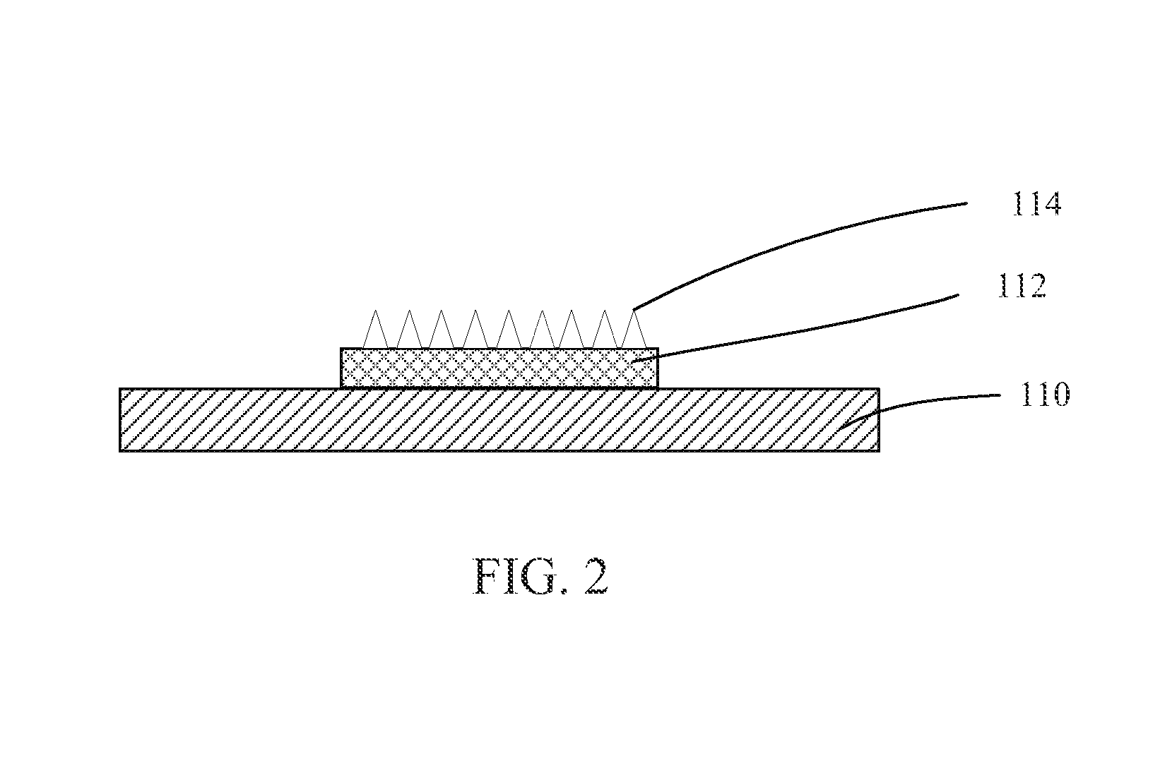
[0010]Referring to FIGS. 1-6, a method for manufacturing a field electron emission source includes the steps of:[0011](a) providing an insulating substrate, depositing a cathode layer on the selective portion of the substrate;[0012](b) patterning a number of emitters on the cathode layer;[0013](c) coating a photoresist layer on the substrate, the cathode layer and the emitters;[0014](d) exposing portions of the photoresist layer to radiation, the portions thereof corresponding to the emitters;[0015](e) forming a mesh structure on the photoresist layer; and[0016](f) removing the exposed portions of photoresist layer, thereby achieving a spacer spaced from the emitters.

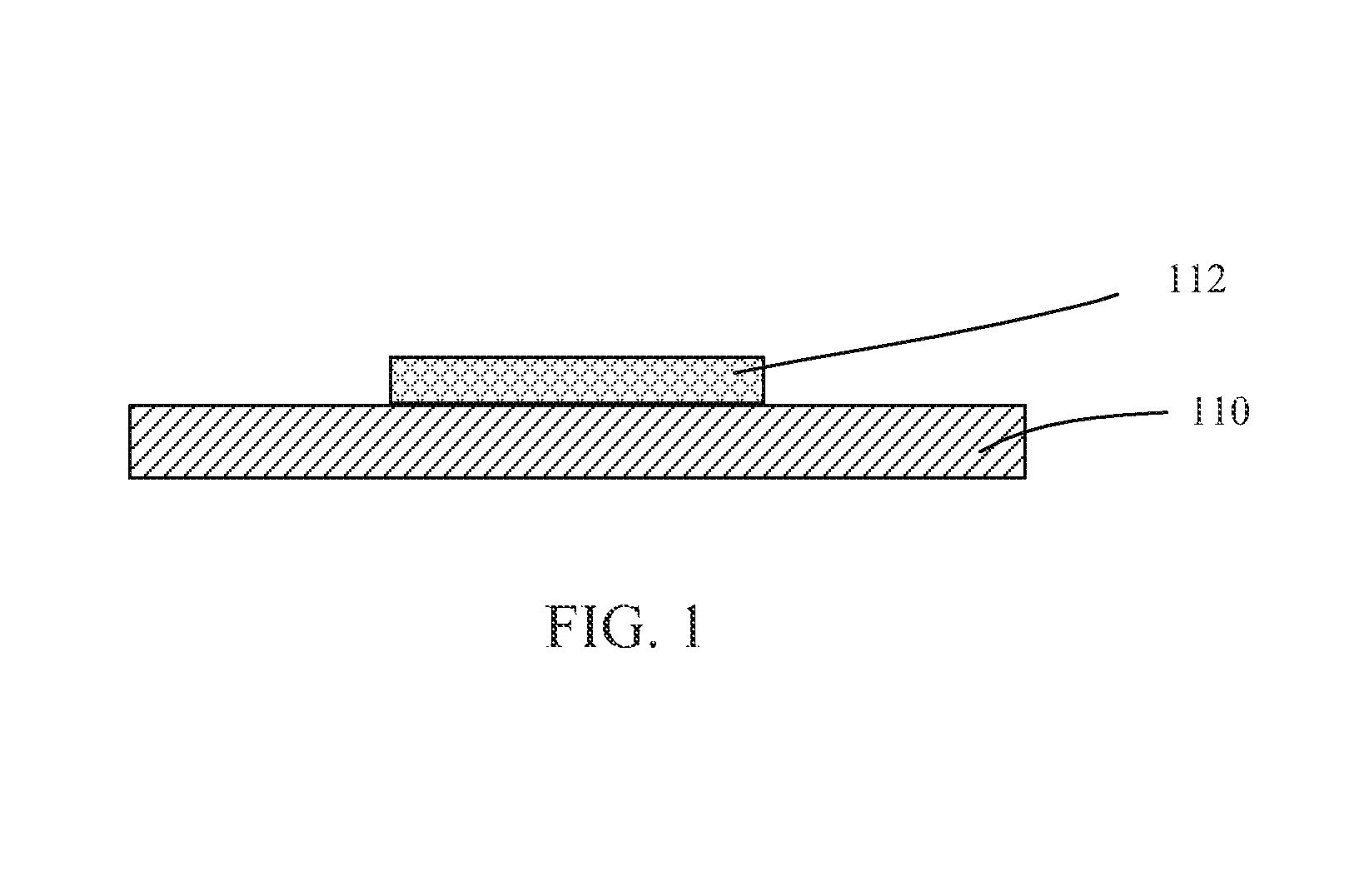
[0017]In step (a), as shown in FIG. 1, an insulating substrate 110 is provided. The insulating substrate 110 can be made of any insulating suitable material, e.g., glass, plastic, and silicon with an insulating layer formed thereon. The insulating substrate 110 can also be a substrate covered with an insulating layer. I...


PUM


Abstract

A method for manufacturing a field electron emission source includes: providing an insulating substrate; patterning a cathode layer on at least one portion of the insulating substrate; forming a number of emitters on the cathode layer; coating a photoresist layer on the insulating substrate, the cathode layer and the emitters; exposing predetermined portions of the photoresist layer to radiation, wherein the exposed portions are corresponding to the emitters; forming a mesh structure on the photoresist layer; and removing the exposed portions of photoresist layer. The method can be easily performed and the achieved the field electron emission source has a high electron emission efficiency.

Description

BACKGROUND[0001]1. Field of the Invention[0002]The present invention relates to a field electron emission source.[0003]2. Discussion of Related Art[0004]Field emission displays (FEDs) are relatively new, rapidly developing flat panel display technologies. FEDs are based on emission of electrons in a vacuum, and light emitted by electrons emitted from micron-sized tips in a strong electric field, accelerating, and colliding with a fluorescent material. FEDs are thin and light with high brightness. Compared to conventional technologies, e.g., cathode-ray tube (CRT) and liquid crystal display (LCD) technologies, FEDs are superior in having a wider viewing angle, lower energy consumption, a smaller size, and a higher quality display. A field electron emission source is an essential component in the FEDs.[0005]The field electron emission source operates in a vacuum environment, where an electrical field is applied to the emitters to generate electrons. The emitters are connected to a cat...

Claims


Application Information

Patent Timeline
Patent Type & Authority Patents(United States)
IPC IPC(8): H01J1/46H01J19/38H01J19/40H01J17/12H01J21/10H01J1/52H01J17/04
CPCH01J1/304H01J3/021H01J9/025H01J31/127H01J2201/30484H01J2201/30492H01J2201/30496H01J2203/0272
Inventor QIAN, LILIU, LIANGFAN, SHOU-SHAN
Owner TSINGHUA UNIV
Why Eureka
Try Eureka