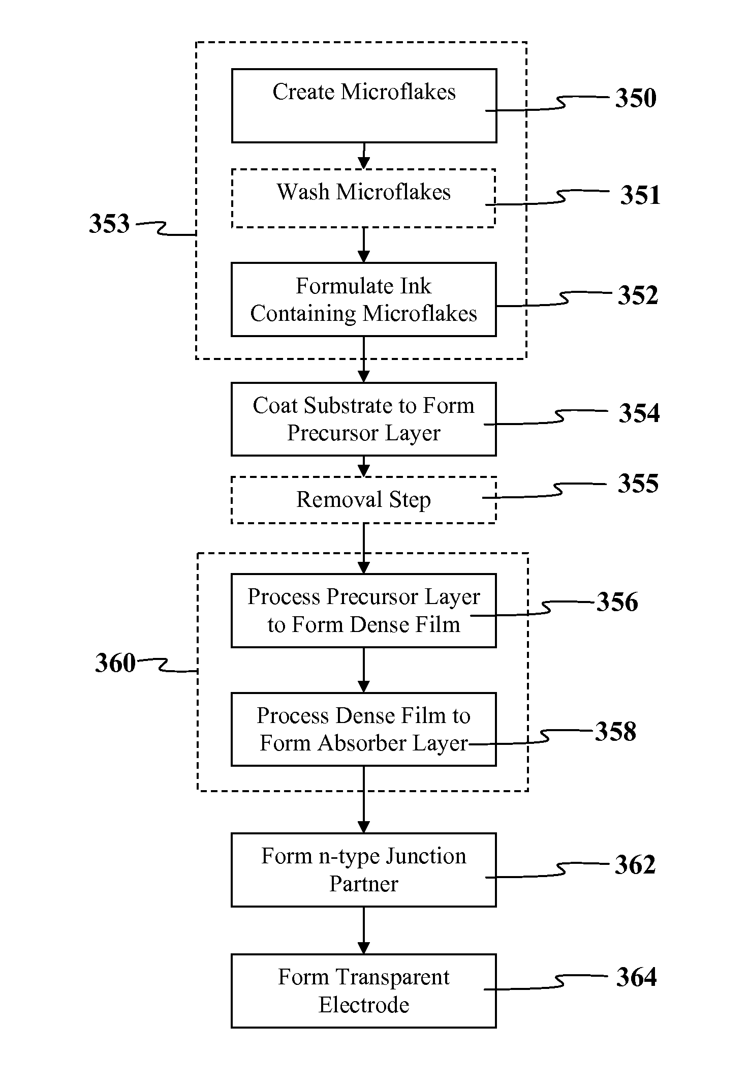
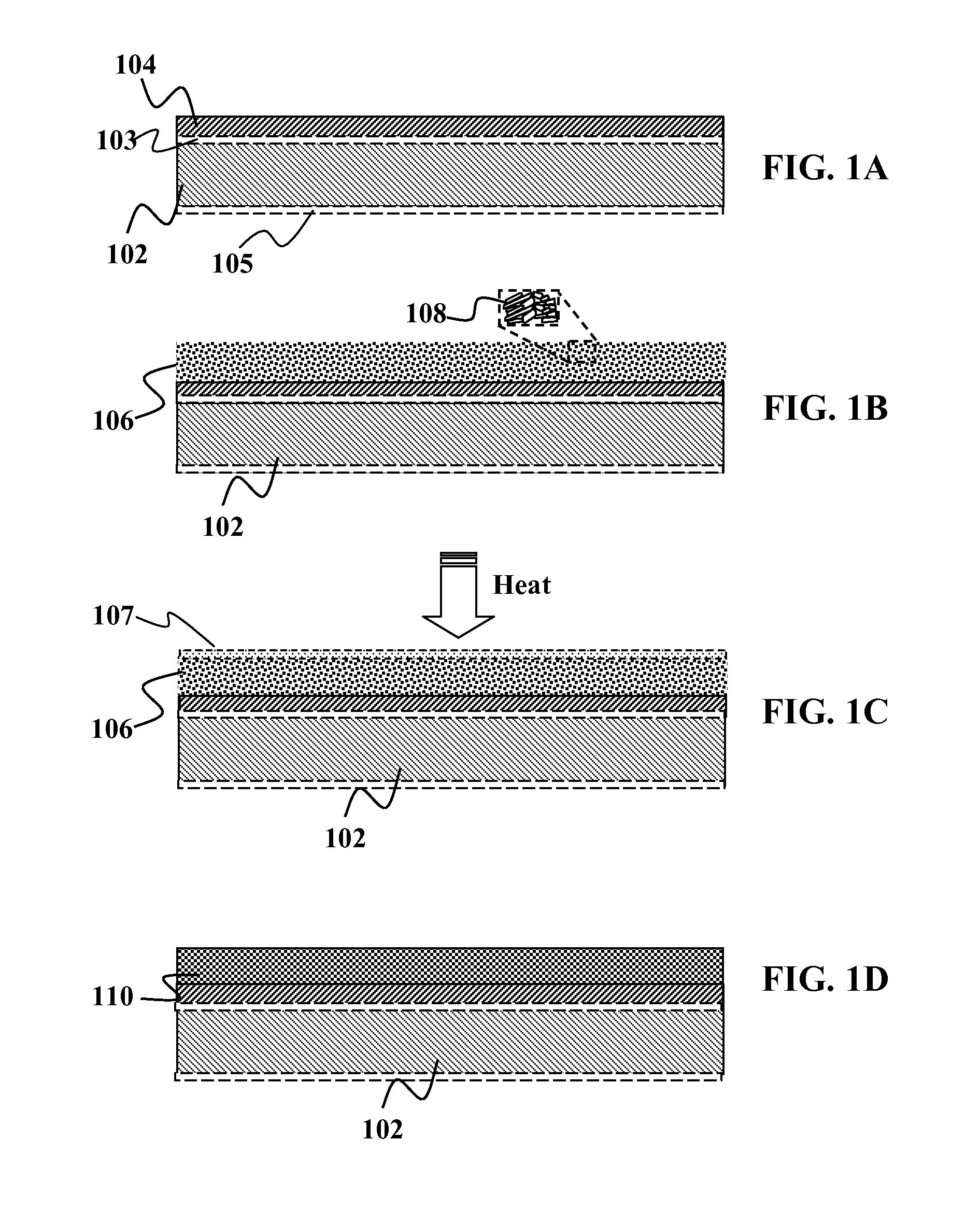
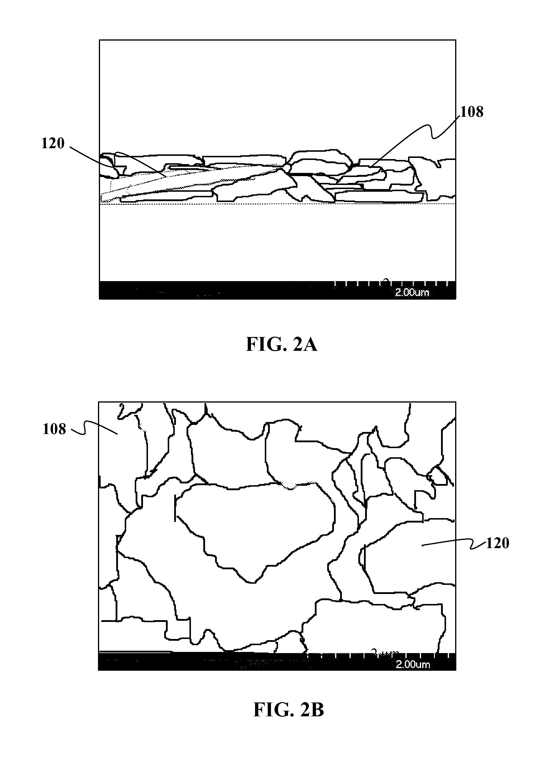
High-throughput printing of semiconductor precursor layer from inter-metallic microflake particles
a technology of intermetallic microflake particles and semiconductor precursor layers, applied in the field of semiconductor precursor layer printing, to achieve the effect of simplifying and facilitating creation
- Summary
- Abstract
- Description
- Claims
- Application Information
AI Technical Summary
Benefits of technology
Problems solved by technology
Method used
Image

Examples
Embodiment Construction
[0075]It is to be understood that both the foregoing general description and the following detailed description are exemplary and explanatory only and are not restrictive of the invention, as claimed. It may be noted that, as used in the specification and the appended claims, the singular forms “a”, “an” and “the” include plural referents unless the context clearly dictates otherwise. Thus, for example, reference to “a material” may include mixtures of materials, reference to “a compound” may include multiple compounds, and the like. References cited herein are hereby incorporated by reference in their entirety, except to the extent that they conflict with teachings explicitly set forth in this specification.
[0076]In this specification and in the claims which follow, reference will be made to a number of terms which shall be defined to have the following meanings:
[0077]“Optional” or “optionally” means that the subsequently described circumstance may or may not occur, so that the des...
PUM
| Property | Measurement | Unit |
|---|---|---|
| grain sizes | aaaaa | aaaaa |
| grain sizes | aaaaa | aaaaa |
| grain sizes | aaaaa | aaaaa |
Abstract
Description
Claims
Application Information
 - R&D
- Intellectual Property
- Life Sciences
- Materials
- Tech Scout
- Unparalleled Data Quality
- Higher Quality Content
- 60% Fewer Hallucinations
Browse by: Latest US Patents, China's latest patents, Technical Efficacy Thesaurus, Application Domain, Technology Topic, Popular Technical Reports.
© 2025 PatSnap. All rights reserved.Legal|Privacy policy|Modern Slavery Act Transparency Statement|Sitemap|About US| Contact US: help@patsnap.com