Semiconductor device having a groove and a junction termination extension layer surrounding a guard ring layer
a technology of junction termination and extension layer, which is applied in the direction of semiconductor devices, semiconductor/solid-state device details, electrical equipment, etc., can solve the problem of significant degradation of break-down voltag
- Summary
- Abstract
- Description
- Claims
- Application Information
AI Technical Summary
Benefits of technology
Problems solved by technology
Method used
Image
Examples
first embodiment
[0021
[0022]In the present embodiment, as an example of a semiconductor device according to the present invention, the structure of a Schottky barrier diode and a method of manufacturing the same will be described.
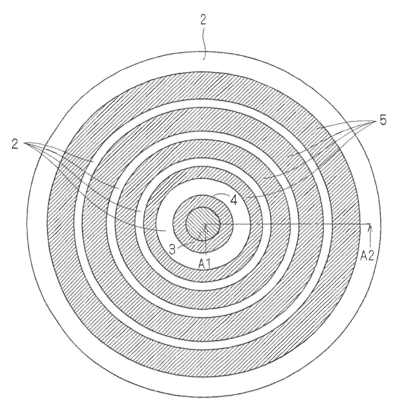
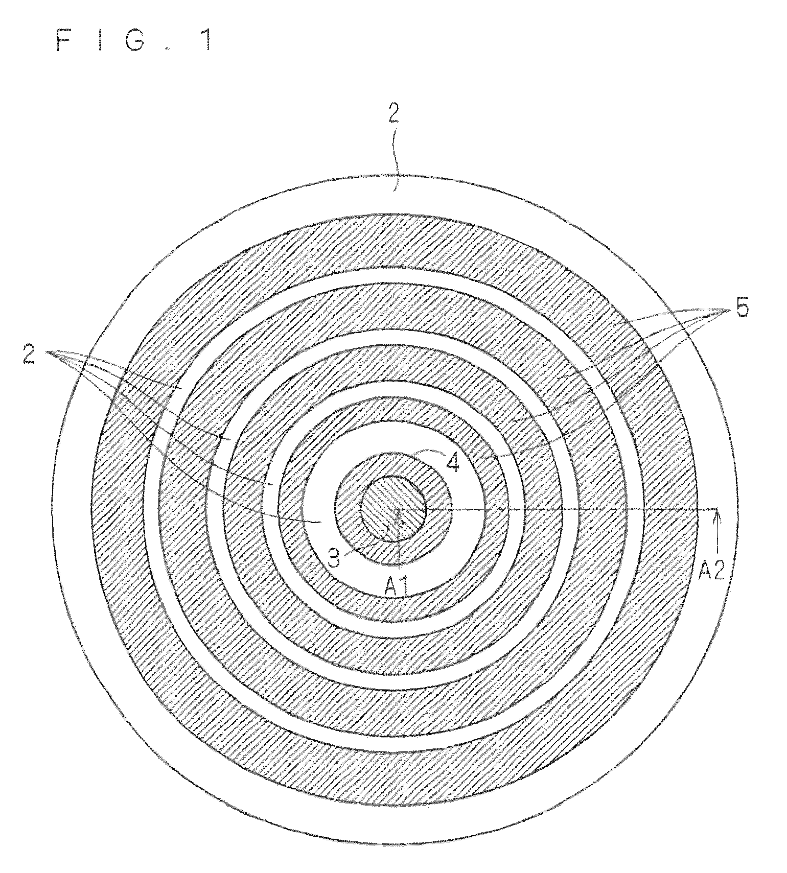
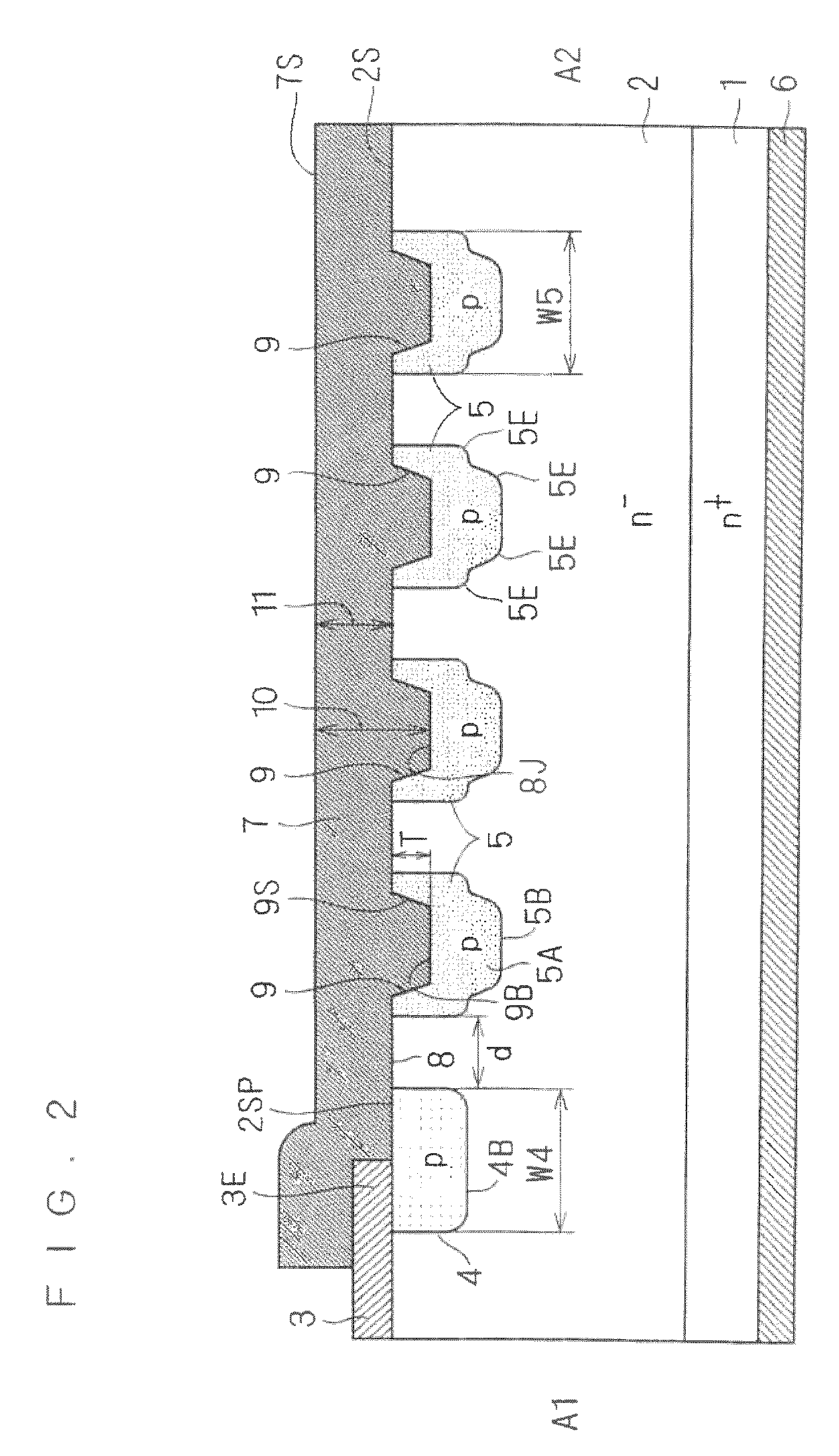
[0023]FIG. 1 is a top view showing the semiconductor device according to the present embodiment. Further, FIG. 2 is a vertical cross-sectional view taken along a line A1-A2 of the top view of FIG. 1. Hereinafter, each cross-sectional view of the semiconductor device described in the present embodiment is assumed to be the vertical cross-sectional view taken along the line A1-A2 of the top view of FIG. 1 of the semiconductor device. Note that for the sake of convenience, an insulating film 7 and grooves 9 disposed correspondingly to respective JTE layers 5, which are shown in FIG. 2, are not shown in FIG. 1.
[0024]The termination structure of the Schottky barrier diode shown in FIG. 2 includes: (1) an n− type semiconductor layer (corresponding to a first conductivity type sem...
first modification
[0048
[0049]FIG. 4 is a vertical cross-sectional view showing a configuration of a semiconductor device according to a first modification of the first embodiment (FIG. 2). The semiconductor device shown in FIG. 4 is different from the semiconductor device shown in FIG. 2 only in that the JTE layer is not formed in the portion directly below the lateral surface 9S of each groove 9 but the JTE layer 5 is formed from the bottom 9B of each groove 9 toward an inside of the n− type semiconductor layer 2. The other structure is similar to the corresponding structure shown in FIG. 2, and detailed description of other reference symbols are omitted.
[0050]Also in the present modification, as in the first embodiment, the distance between the electric field concentration portion (corner portion) of each JTE layer 5 and the surface 2S of the n− type semiconductor layer 2 in which the grooves 9 are not formed is larger than that of the structure of the conventional example shown in FIG. 9. Accordin...
second modification
[0051
[0052]FIG. 5 is a vertical cross-sectional view showing a configuration of a semiconductor device according to a second modification of the first embodiment (FIG. 2). The semiconductor device shown in FIG. 5 is different from the semiconductor device shown in FIG. 2 only in that a depth TP, from the surface 2S of the n− type semiconductor layer 2, of a bottom of a groove 9P among a plurality of grooves 9 that is positioned at the farthest position from or on the outermost side from the GR layer 4 is the largest among the depths T of the bottoms of the other grooves 9a, 9b and 9c (TP>T). Note that other structure is the same as the corresponding structure of the semiconductor device of FIG. 2, and thus the above-mentioned effect produced in the first embodiment is obtained similarly in the present embodiment.
[0053]In the respective JTE layers 5, thicknesses from the bottom of the corresponding groove 9 to the bottoms 5B and 5BP of the respective JTE layers are set to be the same...
PUM
 Abstract
Description
Claims
Application Information
 - R&D
- Intellectual Property
- Life Sciences
- Materials
- Tech Scout
- Unparalleled Data Quality
- Higher Quality Content
- 60% Fewer Hallucinations
Browse by: Latest US Patents, China's latest patents, Technical Efficacy Thesaurus, Application Domain, Technology Topic, Popular Technical Reports.
© 2025 PatSnap. All rights reserved.Legal|Privacy policy|Modern Slavery Act Transparency Statement|Sitemap|About US| Contact US: help@patsnap.com


