
Photoelectrochemical etching for laser facets

a technology of photoelectrochemical and laser facets, applied in the direction of lasers, semiconductor lasers, lasers, etc., can solve the problems of not being able to form cleaved facets, formation of smooth facets, and inability to form smooth facets

Inactive Publication Date: 2012-09-11
RGT UNIV OF CALIFORNIA
View PDF7 Cites 3 Cited by
  • Summary
  • Abstract
  • Description
  • Claims
  • Application Information

AI Technical Summary

Benefits of technology

PEC etching enables the formation of smooth, controlled laser facets with reduced ion damage, improving the quality and performance of GaN-based lasers, particularly for semipolar orientations where cleavage planes are absent, and allowing for precise angle determination by adjusting the light direction.

Problems solved by technology

One of the main difficulties in the fabrication of GaN-based laser structures is the formation of smooth facets that are not compromised by ion damage.
It is also not possible to form cleaved facets when the structure is grown on a non-lattice matched substrate, such as GaN on sapphire.
This technique has not yet been applied to laser facets in the GaN material system because of the difficulty in etching through thick p-type AlGaN layers, which are required for both electrical injection and cladding (carrier and optical confinement) in most laser designs.

Method used


Image

  • Photoelectrochemical etching for laser facets
  • Photoelectrochemical etching for laser facets
  • Photoelectrochemical etching for laser facets

Examples


Embodiment Construction

[0031]In the following description of the preferred embodiment, reference is made to the accompanying drawings which form a part hereof, and in which is shown by way of illustration a specific embodiment in which the invention may be practiced. It is to be understood that other embodiments may be utilized and structural changes may be made without departing from the scope of the present invention.

TECHNICAL DESCRIPTION

[0032]Two concepts are necessary for the present invention:

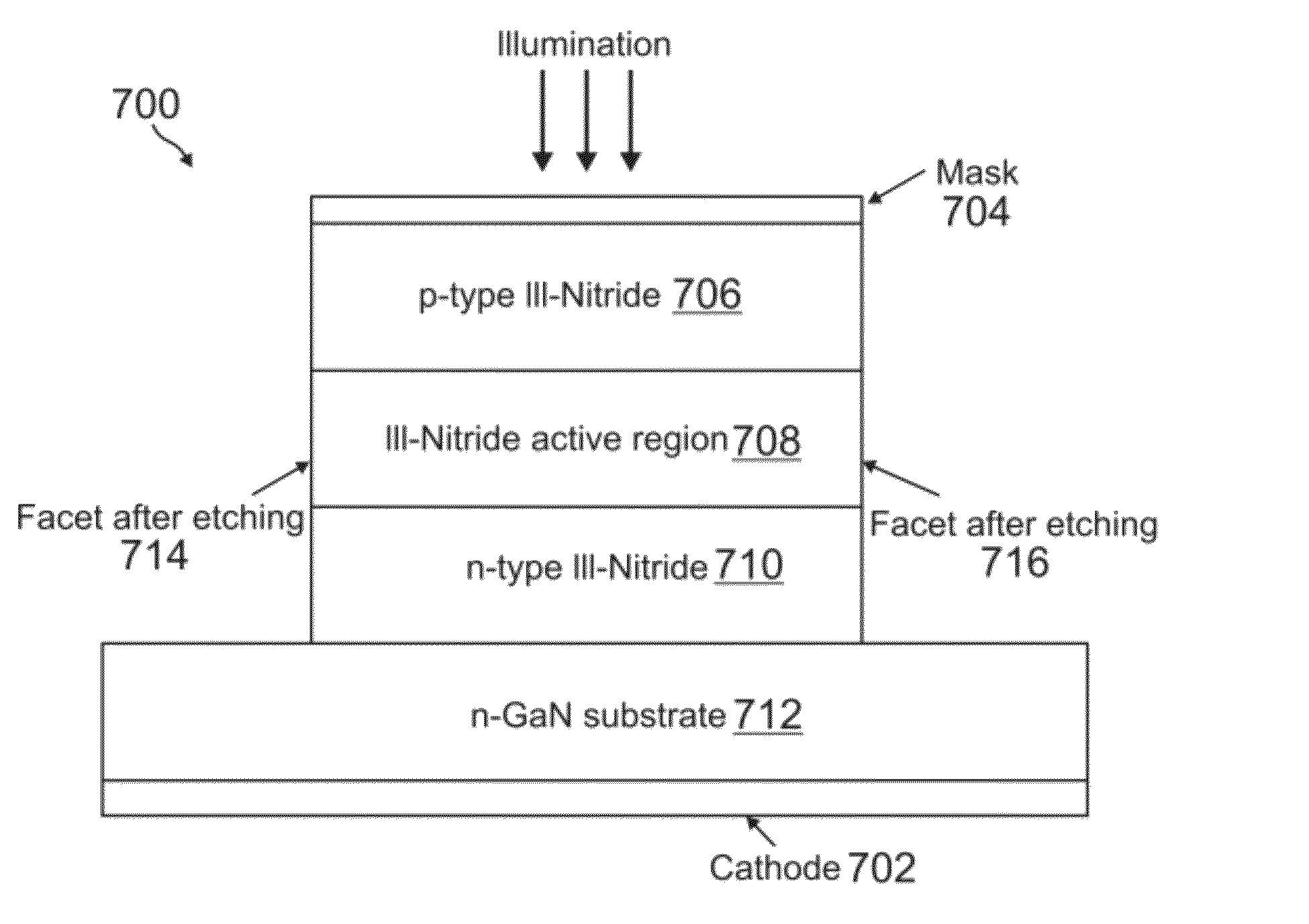
[0033](1) the ability to etch deep, anisotropic trenches with smooth sidewalls in GaN using PEC etching (which was developed using m-plane GaN substrates); and

[0034](2) the ability to PEC etch p-type semiconductors such as p-type GaN and p-type AlGaN, as described in U.S. Utility application Ser. No. 12 / 464,723, filed on May 12, 2009, by Adele Tamboli, Evelyn L. Hu, Mathew C. Schmidt, Shuji Nakamura, and Steven P. DenBaars, entitled “PHOTOELECTROCHEMICAL ETCHING OF P-TYPE SEMICONDUCTOR HETEROSTRUCTURES,” which a...


PUM

PropertyMeasurementUnit
concentrationaaaaaaaaaa
etch rateaaaaaaaaaa
morphologyaaaaaaaaaa

Abstract

A method for fabricating a semiconductor laser device, by etching facets using a photoelectrochemical (PEC) etch, so that the facets are sufficiently smooth to support optical modes within a cavity bounded by the facets.

Description

CROSS REFERENCE TO RELATED APPLICATIONS[0001]This application claims the benefit under 35 U.S.C. Section 119(e) of the following co-pending and commonly-assigned application:[0002]U.S. Provisional Application Ser. No. 61 / 148,679, filed on Jan. 30, 2009, by Adele C. Tamboli, Evelyn L. Hu, Steven P. DenBaars and Arpan Chakraborty, entitled “PHOTOELECTROCHEMICAL ETCHING FOR LASER FACETS,”;[0003]which application is incorporated by reference herein.[0004]This application is related to the following co-pending and commonly-assigned U.S. patent applications:[0005]U.S. Utility application Ser. No. 12 / 464,723, filed on May 12, 2009, by Adele Tamboli, Evelyn L. Hu, Mathew C. Schmidt, Shuji Nakamura, and Steven P. DenBaars, entitled “PHOTOELECTROCHEMICAL ETCHING OF P-TYPE SEMICONDUCTOR HETEROSTRUCTURES,” which application claims the benefit under 35 U.S.C. Section 119(e) of U.S. Provisional Application Ser. No. 61 / 052,421, filed on May 12, 2008, by Adele Tamboli, Evelyn L. Hu, Mathew C. Schmi...

Claims


Application Information

Patent Timeline
Patent Type & Authority Patents(United States)
IPC IPC(8): H01L21/302H01L21/461
CPCH01L21/3063H01S5/0201H01S5/0203H01S5/021H01S5/32341H01L21/306H01S5/00
Inventor TAMBOLI, ADELE C.HU, EVELYN L.DENBAARS, STEVEN P.CHAKRABORTY, ARPAN
Owner RGT UNIV OF CALIFORNIA
Learn More