
Advanced low k cap film formation process for nano electronic devices

a technology of nano electronic devices and nano caps, applied in the direction of coatings, basic electric elements, chemical vapor deposition coatings, etc., can solve the problems of limiting the use of sicn/sub>x/sub>h films, cracking and delamination of dielectric materials and metal films, and affecting the overall effective capacitance of the structure, etc., to achieve the effect of reducing the overall effective capacitance, low cost and high stability

Active Publication Date: 2012-07-03
GLOBALFOUNDRIES INC
View PDF8 Cites 1 Cited by
  • Summary
  • Abstract
  • Description
  • Claims
  • Application Information

AI Technical Summary

Benefits of technology

The carbon-rich silicon carbide-like film reduces overall capacitance, enhances device performance, and maintains stability during post-deposition treatments, preventing cracking and delamination, thus addressing the limitations of existing SiCNxH films.

Problems solved by technology

Under certain circumstances, semiconductor chips may be subjected to external stresses, either during the manufacture or packaging of the chips, or when the packaged chips are mounted or installed in an electronic system for subsequent use.
Occasionally, such external stresses can cause cracking and delamination of dielectric materials and metal films embedded in the dielectric materials.
Difficulties reside in finding appropriate materials and manufacturing processes which permit copper metal lines to be utilized in certain types of low k dielectric materials, particularly when high stress conditions are present.
This change in stress of prior art SiCNxH films under subsequent post processing steps causes significant cracking and thus limits the use of SiCNxH films.

Method used


Image

  • Advanced low k cap film formation process for nano electronic devices
  • Advanced low k cap film formation process for nano electronic devices
  • Advanced low k cap film formation process for nano electronic devices

Examples


example 1

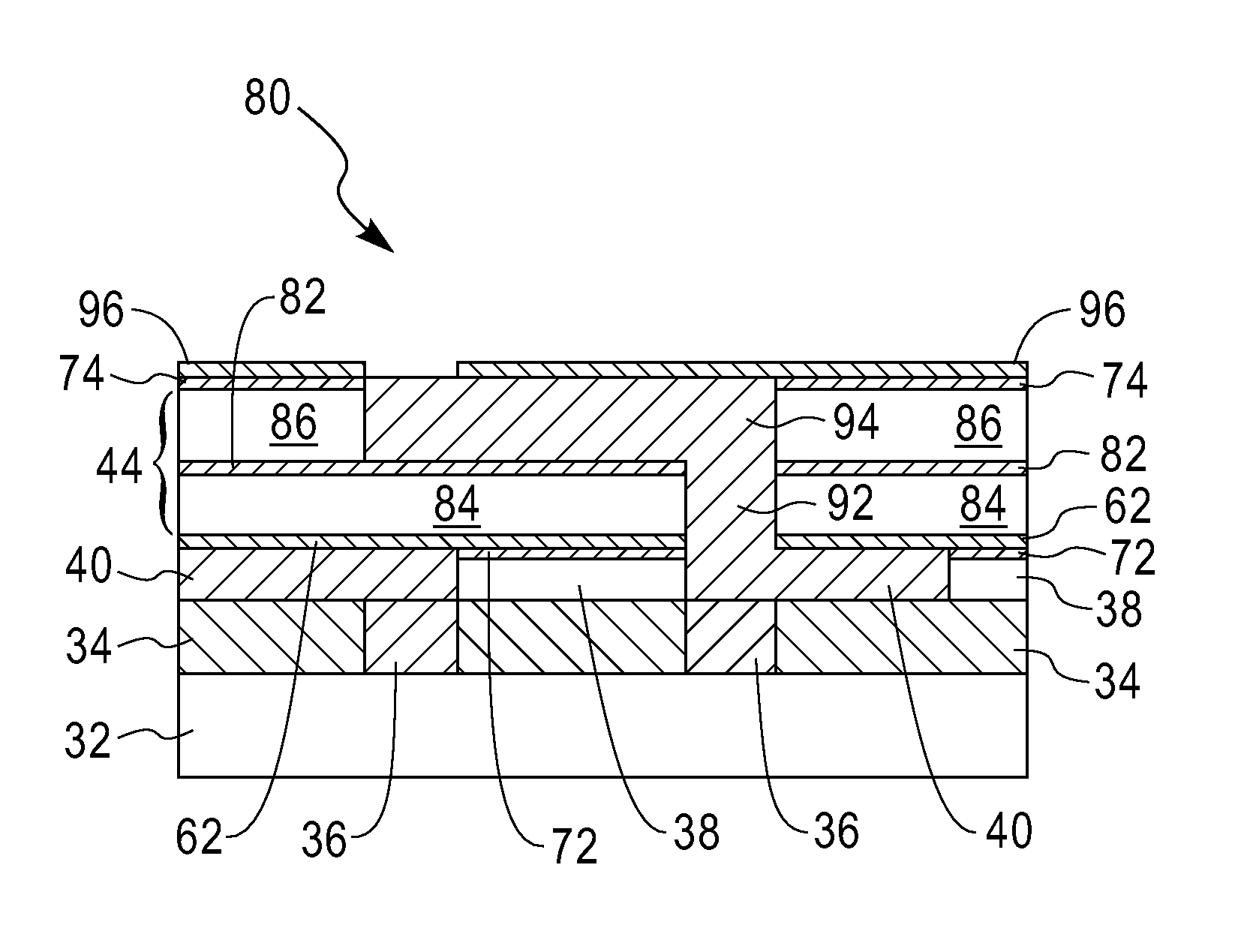
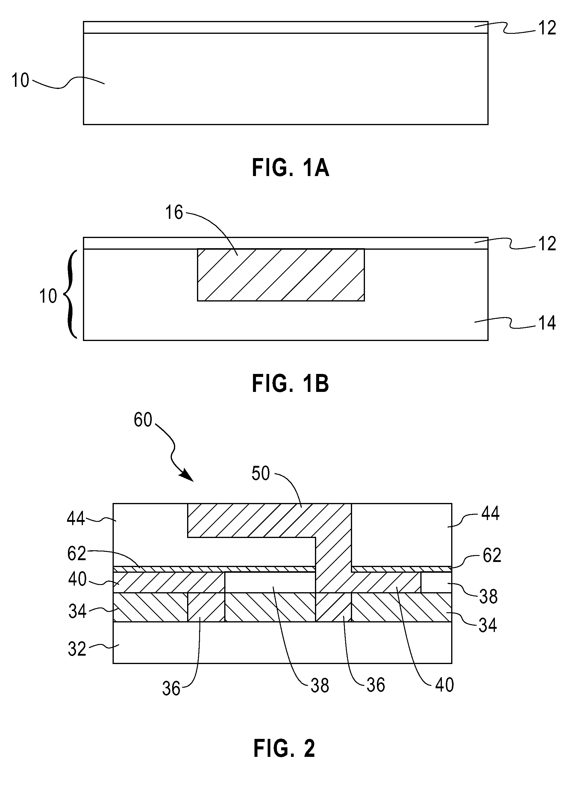
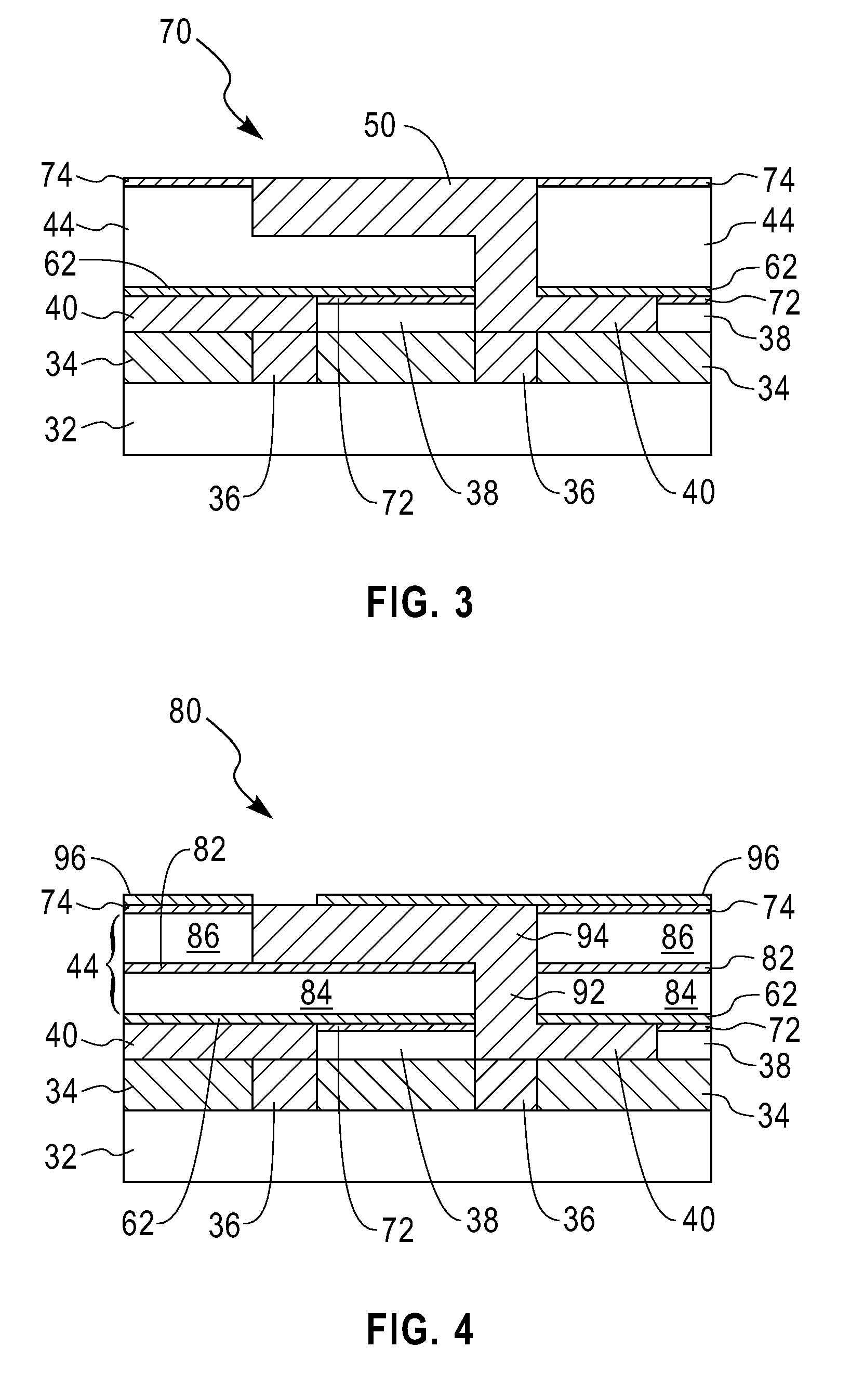
[0074]In this example, a low k dielectric cap film was deposited on a Si wafer utilizing the method of the present application described above. In particular, a low k dielectric film including atoms of Si, C and H was deposited by plasma enhanced chemical vapor deposition (PECVD) utilizing a plasma based on the precursor dimethylsilacyclopentane carried in helium. The as deposited film was mostly carbon rich in composition based on a 6:1 C:Si ratio of the original precursor The deposited film had a dielectric constant of about 2.6-3.6 and it was stable during a subsequent post deposition UV cure treatment step and still maintained compressive stress.

example 2

[0075]In this example, a low k dielectric cap film was deposited on a Si wafer utilizing the method of the present application described above. In particular, a low k dielectric film including atoms of Si, C and H was deposited by plasma enhanced chemical vapor deposition (PECVD) utilizing a plasma based on the precursors dimethylsilacyclopentane and NH3 carried in helium. The as deposited film was carbon rich in composition. The deposited film had a dielectric constant of about 3.5-4.5 depending on the nitrogen concentration and it was stable during a subsequent post UV deposition treatment step and still maintain compressive stress.

example 3

[0076]In this example, a low k dielectric cap film was deposited on a Si wafer utilizing the method of the present application described above but in a two layer deposition scheme. The bottom layer was deposited in particular, a low k dielectric film including atoms of Si, C and H was deposited by plasma enhanced chemical vapor deposition (PECVD) utilizing a plasma based on the precursors dimethylsilacyclopentane and NH3 carried in helium to form a SiCxNyHz film. The top layer in particular, a even low k dielectric film including atoms of Si, C and H was deposited by plasma enhanced chemical vapor deposition (PECVD) utilizing a plasma based on the precursor dimethylsilacyclopentane carried in helium to form a SiCHz film. The as deposited bilayer film was mostly carbon rich in composition based on a 6:1 C:Si ratio of the original precursor. The deposited bilayer film had a dielectric constant of about 2.8-4.0 and it was stable during a subsequent post deposition UV cure treatment ste...


PUM

PropertyMeasurementUnit
dielectric constantaaaaaaaaaa

Abstract

A carbon-rich silicon carbide-like dielectric film having a carbon concentration of greater than, or equal to, about 30 atomic % C and a dielectric constant of less than, or equal to, about 4.5 is provided. In some embodiments, the dielectric film may optionally include nitrogen. When nitrogen is present, the carbon-rich silicon carbide-like dielectric film has a concentration nitrogen that is less than, or equal, to about 5 atomic % nitrogen. The carbon-rich silicon carbide-like dielectric film can be used as a dielectric cap layer in an interconnect structure. The inventive dielectric film is highly robust to UV curing and remains compressively stressed after UV curing. Moreover, the inventive dielectric film has good oxidation resistance and prevents metal diffusion into an interconnect dielectric layer. The present invention also provides an interconnect structure including the inventive dielectric film as a dielectric cap. A method of fabricating the inventive dielectric film is also provided.

Description

FIELD OF THE INVENTION[0001]The present invention relates to semiconductor interconnect structures for nano integrated circuit devices and a process for fabricating the same. More particularly, the present invention relates to a low k dielectric film that serves as a dielectric cap of an interconnect structure and a method of fabricating the low k dielectric film.BACKGROUND OF THE INVENTION[0002]Integrated circuits (ICs) typically include a plurality of semiconductor devices and interconnect wiring. Networks of metal interconnect wiring typically connect the semiconductor devices from the semiconductor portion of the substrate. Multiple levels of metal interconnect wiring above the semiconductor portion of the substrate are connected together to form a back-end-of-the-line (“BEOL”) interconnect structure. Within such a structure, metal lines run parallel to the substrate and conductive vias run perpendicular to the substrate; the conductive vias typically interconnect the different ...

Claims


Application Information

Patent Timeline
Patent Type & Authority Patents(United States)
IPC IPC(8): H01L23/58H01L23/48
CPCC23C16/325C23C16/56H01L21/76825H01L21/02263H01L21/76829H01L21/76832H01L21/76834H01L21/76826
Inventor GRILL, ALFREDHERMAN, JOSHUA L.NGUYEN, SONRYAN, E. TODDSHOBHA, HOSADURGA K.
Owner GLOBALFOUNDRIES INC
Learn More