
Electron microscope for inspecting dimension and shape of a pattern formed on a wafer

a technology of electron microscope and pattern, which is applied in the direction of instruments, television systems, nuclear engineering, etc., can solve the problems of increasing difficulty in ensuring the desired dimension accuracy of the pattern on the wafer, increasing the difficulty of pattern formation, and requiring a tremendous amount of time and labor for investigating the cause of complex problems

Inactive Publication Date: 2012-06-12
HITACHI HIGH-TECH CORP
View PDF23 Cites 1 Cited by
  • Summary
  • Abstract
  • Description
  • Claims
  • Application Information

AI Technical Summary

Benefits of technology

The present invention provides an electron microscope that can efficiently investigate causes of pattern abnormalities on a wafer. The electron microscope has a feature of displaying a microscopic image of a pattern on a photomask and a microscopic image of the pattern on the wafer in a same display condition, allowing for easy comparison and contrast between the two images. This helps to determine which part of the process caused the pattern abnormality on the wafer, which can aid in identifying the root cause of the issue and take appropriate measures to address it. Overall, the invention provides a more efficient and effective tool for analyzing and improving the manufacturing process of semiconductor devices.

Problems solved by technology

Ensuring the desired dimension accuracy of the pattern on the wafer, however, is becoming increasingly difficult because of the following various causes: Complication of the photomask pattern in accompaniment with the OPC, dimension accuracy of the photomask, and further, stability of the fabrication process.
Moreover, the difficulty in the pattern formation has become even more serious because of an increase in pattern data capacity due to the microminiaturization.
However, even if abnormalities of the CD or shape in the pattern have been found out in this way, events which are conceivable as causes for the abnormalities cover a fairly broad range, such as inappropriateness of the OPC, the CD or shape of the photomask, and the fabrication process.
Consequently, a task for investigating the complicated causes necessitates tremendous amount of time and labor.

Method used


Image

  • Electron microscope for inspecting dimension and shape of a pattern formed on a wafer
  • Electron microscope for inspecting dimension and shape of a pattern formed on a wafer
  • Electron microscope for inspecting dimension and shape of a pattern formed on a wafer

Examples


1st embodiment

(1st Embodiment)

[0042]In the present embodiment, the display and comparison are performed between a microscopic image of pattern formed on a wafer by using a photomask and a microscopic image of pattern of the photomask on a quartz substrate, i.e., the original version of the pattern formed on the wafer.

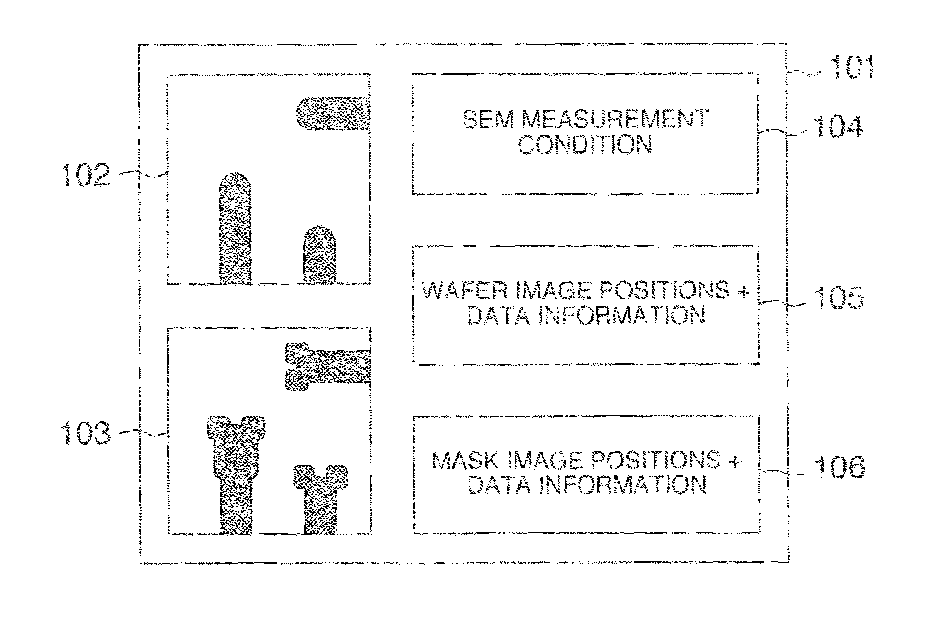
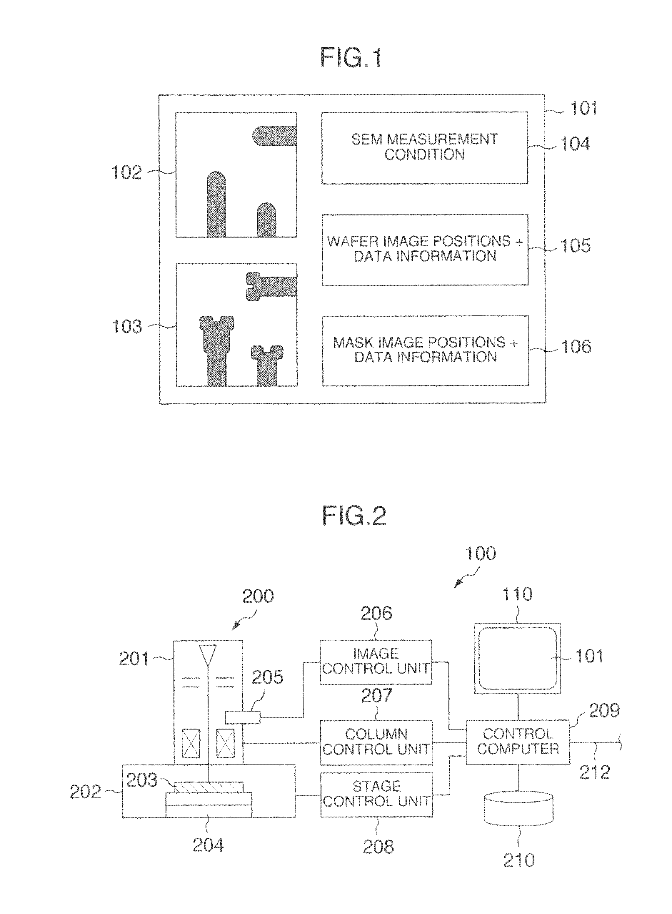
[0043]FIG. 1 is a diagram for illustrating an example of the display screen of the electron microscope according to the first embodiment of the present invention.

[0044]In FIG. 1, within the display screen 101 of a display device 110 (refer to FIG. 2) including, e.g., CRT or LCD, layout is performed with respect to the following display areas each: In an upper-left area of the screen, a display area of a microscopic image (hereinafter, referred to as “image 102”) of pattern formed on a wafer acquired by the electron microscope according to the present embodiment, and, in a lower-left area of the screen, a display area of a microscopic image (hereinafter, referred to as “image 103”) of...

2nd embodiment

(2nd Embodiment)

[0070]In the length-measuring SEM, there exists a method of determining a length-measuring position with CAD pattern data, i.e., design data on the on-wafer pattern, employed as the reference. In this method, a comparison is made between the CAD data and the pattern image acquired by the length-measuring SEM, then making the pass / fail judgment based on data on the dimension difference with the CAD data. The format for the CAD pattern data is GDSII format or OASIS format. In these data formats, a pattern and its position are defined by a polygon whose dimension is substantially equal to that of the on-wafer pattern. Taking advantage of the CAD data in this way makes it unnecessary to register the image data on a length-measuring pattern itself at the time of length measurement. Accordingly, it becomes possible to shorten a time for determining the measurement condition and measurement processing step if the length measurement of the same pattern is not made at a plura...

3rd embodiment

(3rd Embodiment)

[0080]The present embodiment relates to a concrete method for implementing, in the embodiments described hereinbefore, a common management of the pattern information acquired by another electron microscope and the pattern information acquired by the present electron microscope itself. Namely, the photomask pattern image is made related with the data and the CAD data in advance. As a result of this, when an abnormality location is found out at the time of evaluation of the on-wafer pattern, it is made possible to display the photomask pattern image and the CAD pattern outer-shape of the corresponding location with an excellent efficiency. This allows accomplishment of an even higher efficiency in investigating the occurrence causes. The present embodiment is particularly effective when evaluation points on the on-wafer pattern increase in number.

[0081]First, what is needed as information is the recognition of the photomask by which an on-wafer pattern is formed. For t...


PUM


Abstract

There is provided an electron microscope which is capable of making a significant contribution to accomplishment of efficiency in investigating causes for pattern abnormalities found out. The electron microscope including an I / O for capturing image data on a microscopic image acquired by another electron microscope, a computation processing unit for generating a display signal based on the image data on the microscopic image acquired by another electron microscope and captured via the I / O and image data on a microscopic image acquired by the electron microscope itself, in order that the microscopic image acquired by another electron microscope and the microscopic image acquired by the electron microscope itself are displayed at the same scale and under the same display condition, and a display unit for displaying both of the microscopic images based on the display signal from the computation processing unit.

Description

BACKGROUND OF THE INVENTION[0001]The present invention relates to an electron microscope for inspecting dimension and shape of a pattern formed on a wafer.[0002]The shape and dimension of a pattern formed on a wafer and those of a photomask pattern are measured and evaluated using an evaluation tool so as to judge the pass / fail. In the measurement of a critical dimension (which, hereinafter, will be referred to as “CD”) in particular, a scanning electron microscope (hereinafter, referred to as “SEM”) equipped with a length-measuring function is generally used.[0003]Also, in accompaniment with microminiaturization and complication of semiconductor integrated circuits in recent years, an optical proximity correction (hereinafter, referred to as “OPC”) has been getting more and more applied to a photomask pattern. Here, the photomask pattern is used when the pattern of a semiconductor integrated circuit is transferred onto a wafer by a microlithography tool. With respect to the pattern...

Claims


Application Information

Patent Timeline
Patent Type & Authority Patents(United States)
IPC IPC(8): H04N7/18G02B21/00G06K9/00
CPCH01J37/28H01J2237/221H01J2237/2485H01J2237/2816H01J2237/2817
Inventor SATO, HIDETOSHISUTANI, TAKUMICHIHOJO, YUTAKA
Owner HITACHI HIGH-TECH CORP
Learn More