Leadframe

a technology of lead frame and surface mount, which is applied in the direction of semiconductor devices, semiconductor/solid-state device details, electrical apparatus, etc., can solve the problems of failure of visual inspection, significant heat generation of the function die, electrical short circuit, etc., and achieve the effect of reducing or eliminating the vertical offset of the package and reducing the contact of the plating material

Active Publication Date: 2012-03-13
MACRONIX INT CO LTD
View PDF56 Cites 6 Cited by
  • Summary
  • Abstract
  • Description
  • Claims
  • Application Information

AI Technical Summary

Benefits of technology

[0014]Generally, the invention features a leadframe in which at least part of the surface of the die paddle opposite the die mount side (the “back” side) is recessed in relation to the back side of the package. The leadframe may have an upset die paddle, and a mold flow dam ring may be employed to prevent incursion of the encapsulant over the back side of the die paddle; or, the back side of the die paddle may be etched back following encapsulation. Or the die paddle may be provided with a fillister in the back side, defining a rim and a recessed surface. The plating material covers the lower surfaces of the leads and the lower surfaces of the recessed die paddle. The volume of the space defined by the recess is sufficient to accommodate protrusions of the plating material in the recess, to mitigate contact of the plating material with the underlying support during surface mount on a support. Accordingly, vertical offset of the package can be reduced or eliminated, and unwanted contact of the fusible material beneath the die paddle with underlying circuitry in the support can be avoided.

Problems solved by technology

The functioning die can generate a significant amount of heat.
One source of failure in visual inspection is a consequence of the fact that, as the plating material melts, the melted mass tends by cohesion to form an irregular protruding shape.
Or, the support may have unmasked circuit traces underlying the die paddle, and the protruding solder mass on the die paddle may contact these circuit traces and cause an electrical short.
Even in cases where the protruding mass would not in fact interfere with good electrical contact or result in electrical shorting if the package were mounted, the package may nevertheless be rejected for failing visual inspection.

Method used


Image

  • Leadframe
  • Leadframe
  • Leadframe

Examples


Embodiment Construction

[0038]The invention will now be described in further detail by reference to the drawings, which illustrate alternative embodiments of the invention. The drawings are diagrammatic, showing features of the invention and their relation to other features and structures, and are not made to scale. For improved clarity of presentation, in the FIGs. illustrating embodiments of the invention, features corresponding to features shown in other drawings are not all particularly renumbered, although they are all readily identifiable in all the FIGs.

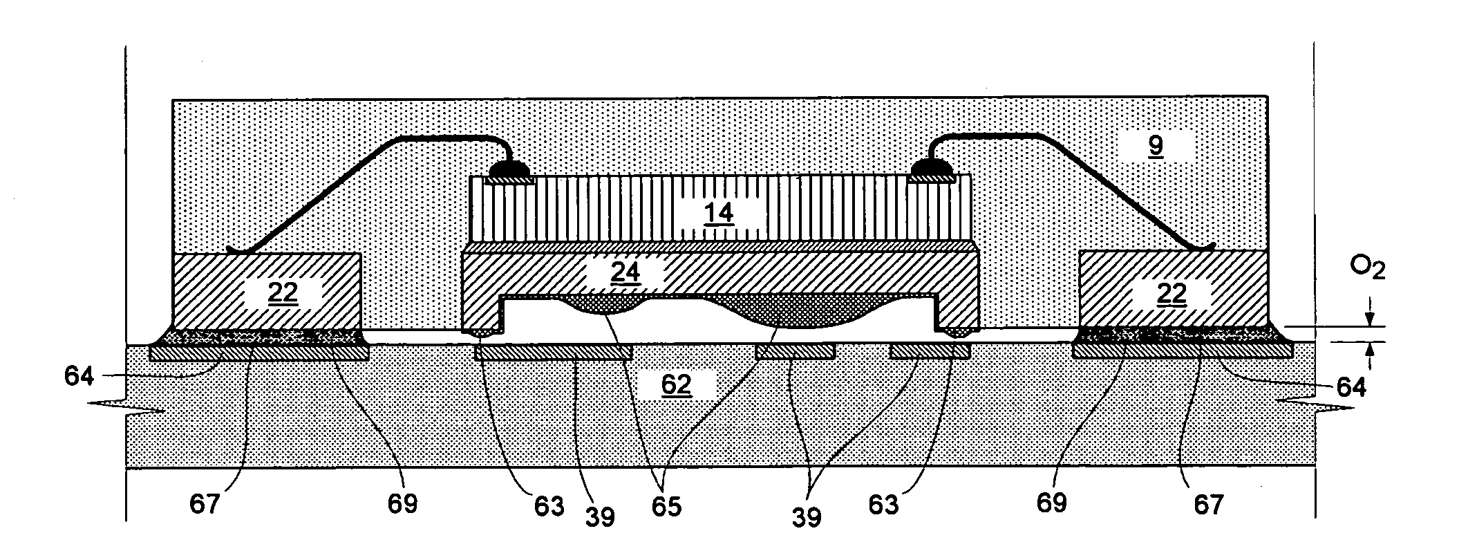
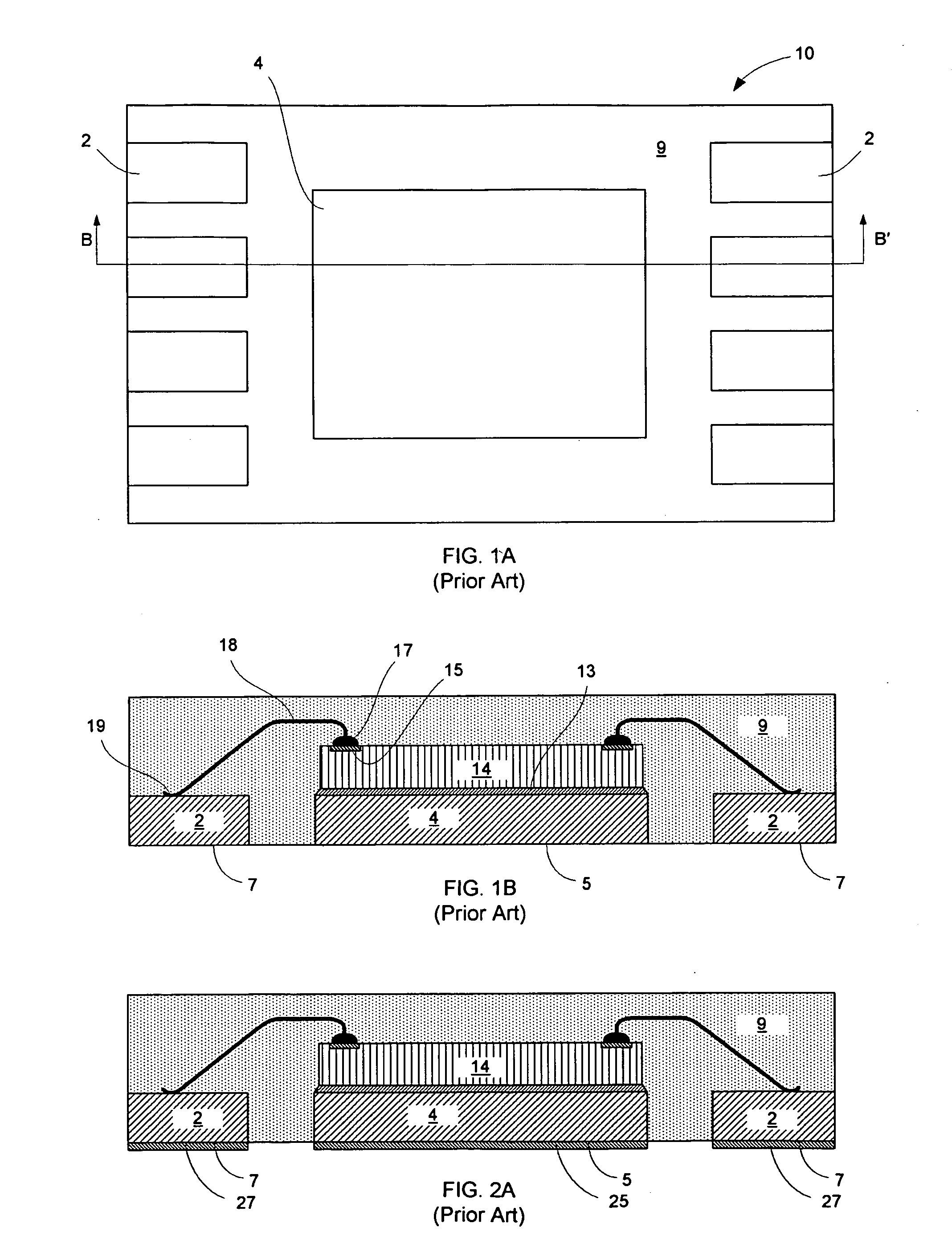
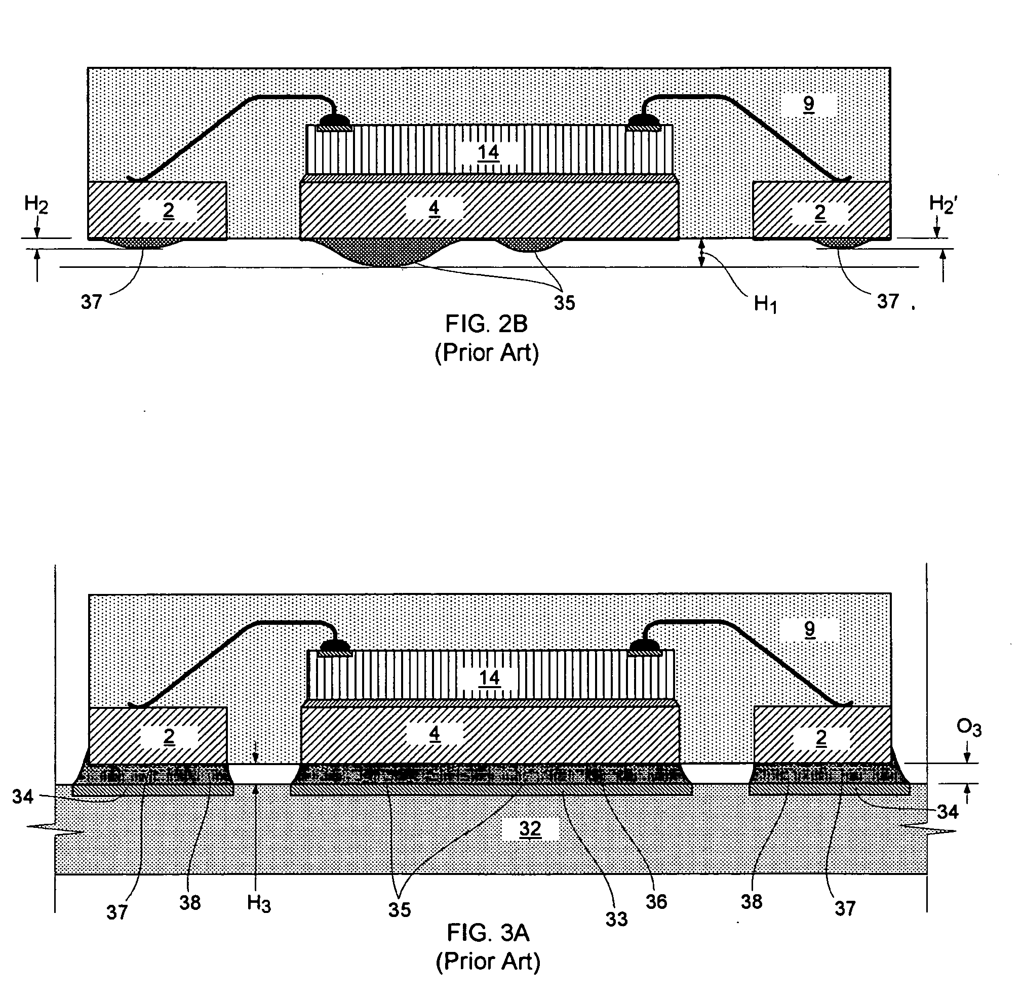
[0039]FIGS. 1A and 1B show a conventional DFN package; FIG. 2A shows the DFN package with plating, ready for testing; and FIG. 2B shows the package following thermal cycling, ready for surface mount. FIG. 3A shows a mounted package, and FIGS. 3B and 3C show two modes of failure that may result from an attempt to mount a conventional plated package onto a support such as a printed circuit board.

[0040]Referring now to FIG. 1A, there is shown generally ...


PUM


Abstract

A leadframe includes a die paddle and leads, in which the back side of the die paddle has a fillister. The fillister defines a rim surrounding a recess, and the recess accommodates protrusion of fusible material. Also, a package includes such a leadframe. Also, a method for making a leadframe includes patterning a sheet of metal to form a die paddle and leads, and forming a fillister in the back side of the die paddle.

Description

BACKGROUND[0001]1. Field of the Invention[0002]This invention relates to semiconductor package Surface Mount Technology (“SMT”) and, particularly, to surface mount of packages having an exposed die paddle surface.[0003]2. Description of Related Art[0004]A conventional leadframe semiconductor die package has a semiconductor die mounted onto and electrically connected to a leadframe. The leadframe, which may be formed by patterning a sheet of electrically conductive metal such as copper, typically includes a die paddle, onto which the die is affixed, and leads, to which the die is electrically connected. The mounted die may be encapsulated or molded, and the leads may project from one or more sidewalls of the molding or encapsulation (a “leaded package”); or the leads may end at one or more of the sidewalls of the molding or encapsulation (a “leadless package” or “no-lead package”).[0005]An encapsulated leadless package is shaped generally as a thin rectangular parallepiped having lar...

Claims


Application Information

Patent Timeline
Patent Type & Authority Patents(United States)
IPC IPC(8): H01L21/00
CPCH01L23/3107H01L23/49503H01L23/49582H01L24/29H01L24/48H01L2224/32245H01L2224/48091H01L2224/48095H01L2224/48247H01L2224/48465H01L2224/73265H01L2924/01029H01L2924/01077H01L2924/01078H01L2924/078H01L2924/181H01L2924/00014H01L2924/00H01L2924/00012H01L2224/45099H01L2224/45015H01L2924/207
Inventor LEE, JUI-CHUNGLIN, PO-HSINLEE, KUN-FENG
Owner MACRONIX INT CO LTD
Why Eureka
Try Eureka