Eureka AIR delivers breakthrough ideas for toughest innovation challenges, trusted by R&D personnel around the world.

Amplifying element and manufacturing method thereof

a manufacturing method and technology of amplifiers, applied in the direction of transducer casings/cabinets/supports, transducers with semiconductor devices/discharge tubes, electric transducers, etc., can solve the problems of low gain, noise generated by each resistance and semiconductor, and complicated circuit configuration of amplifier integrated circuit elements

Active Publication Date: 2012-01-31
SEMICON COMPONENTS IND LLC
View PDF5 Cites 0 Cited by
  • Summary
  • Abstract
  • Description
  • Claims
  • Application Information

AI Technical Summary

Benefits of technology

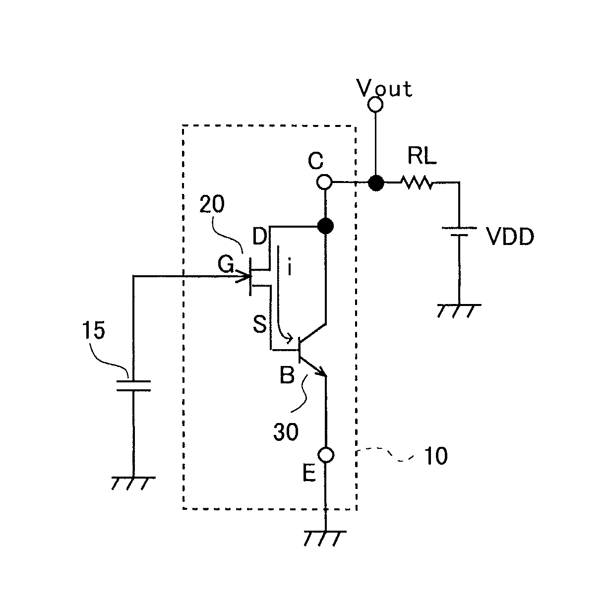
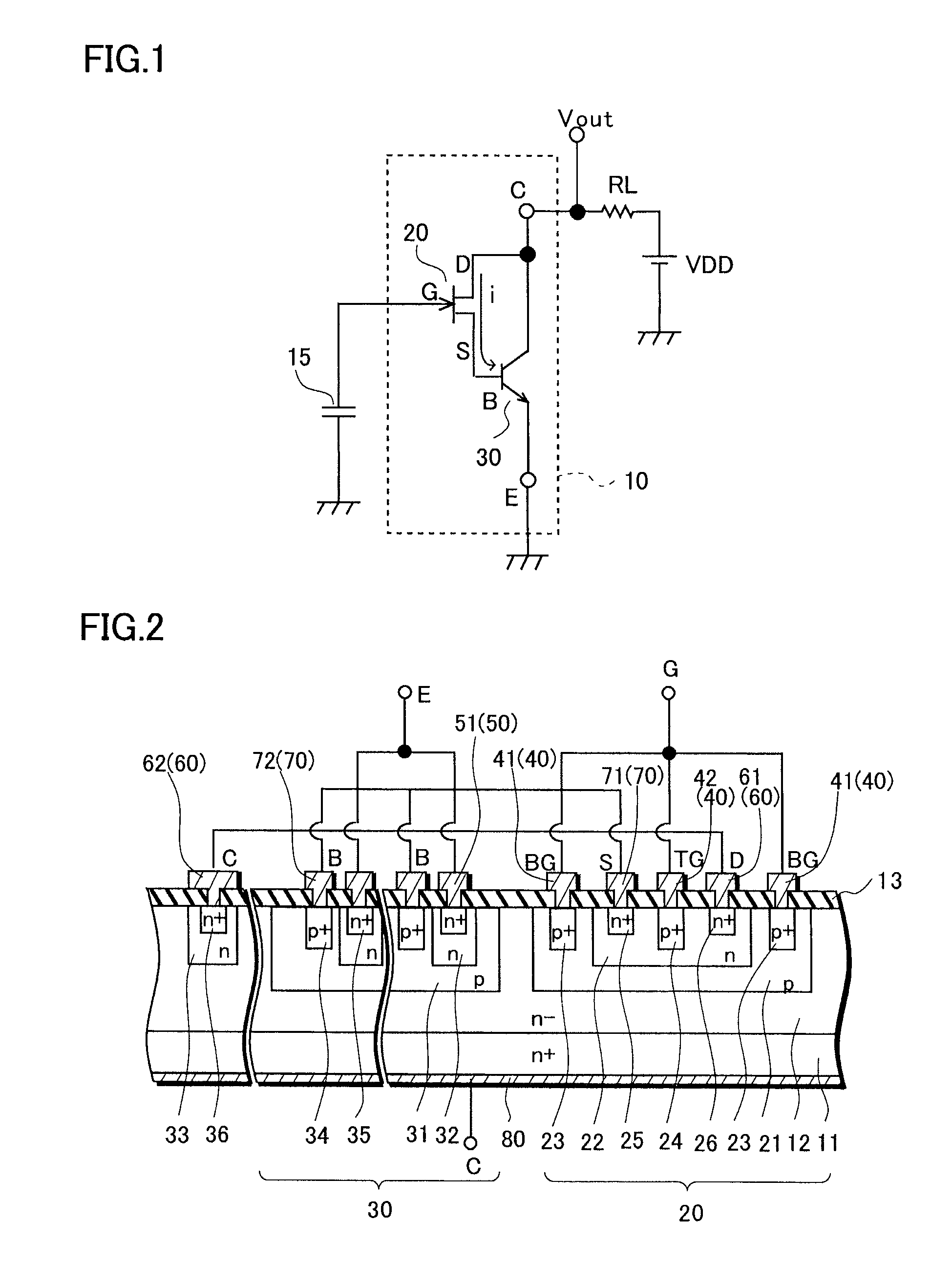
[0018]The invention further provides an electret condenser microphone system that includes an electret condenser microphone having a first terminal and a second terminal and an amplifying element including a semiconductor substrate, a junction field effect transistor formed on the semiconductor substrate and a bipolar transistor formed on the semiconductor substrate. The first terminal of the electret condenser microphone is connected to the gate of the junction filed effect transistor, the source of the junction field effect transistor is connected to the base of the bipolar transistor, and the drain of the junction filed effect transistor is connected to the collector of the bipolar transistor. The system also includes a load resistor connected to the collector of the bipolar transistor.
[0018]The invention further provides an electret condenser microphone system that includes an electret condenser microphone having a first terminal and a second terminal and an amplifying element including a semiconductor substrate, a junction field effect transistor formed on the semiconductor substrate and a bipolar transistor formed on the semiconductor substrate. The first terminal of the electret condenser microphone is connected to the gate of the junction filed effect transistor, the source of the junction field effect transistor is connected to the base of the bipolar transistor, and the drain of the junction filed effect transistor is connected to the collector of the bipolar transistor. The system also includes a load resistor connected to the collector of the bipolar transistor.
[0015]However, in order to decrease the input capacitance Cin as described above, the area of the J-FET has to be reduced. In this case, the J-FET is capable of controlling only a reduced amount of current, thereby producing only a small gain. In other words, the gain and the input capacitance Cin have a trade-off relationship. Thus, the simple and reasonable amplifying element using the J-FET has a limitation in improving the gain.
[0008]The amplifier integrated circuit element has advantages that an appropriate gain of the circuit element can be selectively set by adjusting a circuit constant, and that the amplifier integrated circuit element generally produces a higher gain than the J-FET. However, the amplifier integrated circuit element has a problem of having a complicated circuit configuration and of requiring high costs.
[0018]The invention further provides an electret condenser microphone system that includes an electret condenser microphone having a first terminal and a second terminal and an amplifying element including a semiconductor substrate, a junction field effect transistor formed on the semiconductor substrate and a bipolar transistor formed on the semiconductor substrate. The first terminal of the electret condenser microphone is connected to the gate of the junction filed effect transistor, the source of the junction field effect transistor is connected to the base of the bipolar transistor, and the drain of the junction filed effect transistor is connected to the collector of the bipolar transistor. The system also includes a load resistor connected to the collector of the bipolar transistor.
[0105]Thirdly, the amplification factor of the amplifying element can be appropriately selected according to the amplification factor of the bipolar transistor.
[0017]The method also provides a method of manufacturing an amplifying element to be connected to an electret condenser microphone. The method includes forming a semiconductor layer of a first general conductivity type on a semiconductor substrate of the first general conductivity type, forming in the semiconductor layer a back gate diffusion region and a base region that are of a second general conductivity type, forming a channel region of the first general conductivity type in the back gate diffusion region and an emitter region of the first general conductivity type in the base region, forming a top gate region of the second general conductivity type in the channel region, forming in the channel region a source region and a drain region that are of the first general conductivity type, electrically connecting the source region and the base region, and electrically connecting the drain region and the collector region.
[0010]Since the amplifier integrated circuit element amplifies an input together with input noise, S / N, which is an index of sound quality, is not improved even when the gain is changed. Additionally, the noise is generated from each of resistances and semiconductors. For this reason, having a more complicated circuit configuration than the J-FET with a simple configuration, the amplifier integrated circuit element includes a larger number of noise resources, and accordingly has a lower S / N than the J-FET, in general. Accordingly, it is a common practice to use the amplifier integrated circuit element if high sensitivity is required to be achieved, but to use the J-FET if the required sensitivity is achievable by the J-FET.

Problems solved by technology

However, the amplifier integrated circuit element has a problem of having a complicated circuit configuration and of requiring high costs.
Additionally, the noise is generated from each of resistances and semiconductors.
However, there is a problem that the J-FET alone cannot sufficiently amplify an output, so that the resultant gain is low.
As expressed by the equation of Vin=Cm / (Cm+Cin)VAC, the input voltage Vin of the J-FET in this case becomes smaller as Cm becomes smaller or Cin becomes larger, thereby causing an input loss.
Thus, the simple and reasonable amplifying element using the J-FET has a limitation in improving the gain.

Method used


Image

  • Amplifying element and manufacturing method thereof
  • Amplifying element and manufacturing method thereof
  • Amplifying element and manufacturing method thereof

Examples


Embodiment Construction

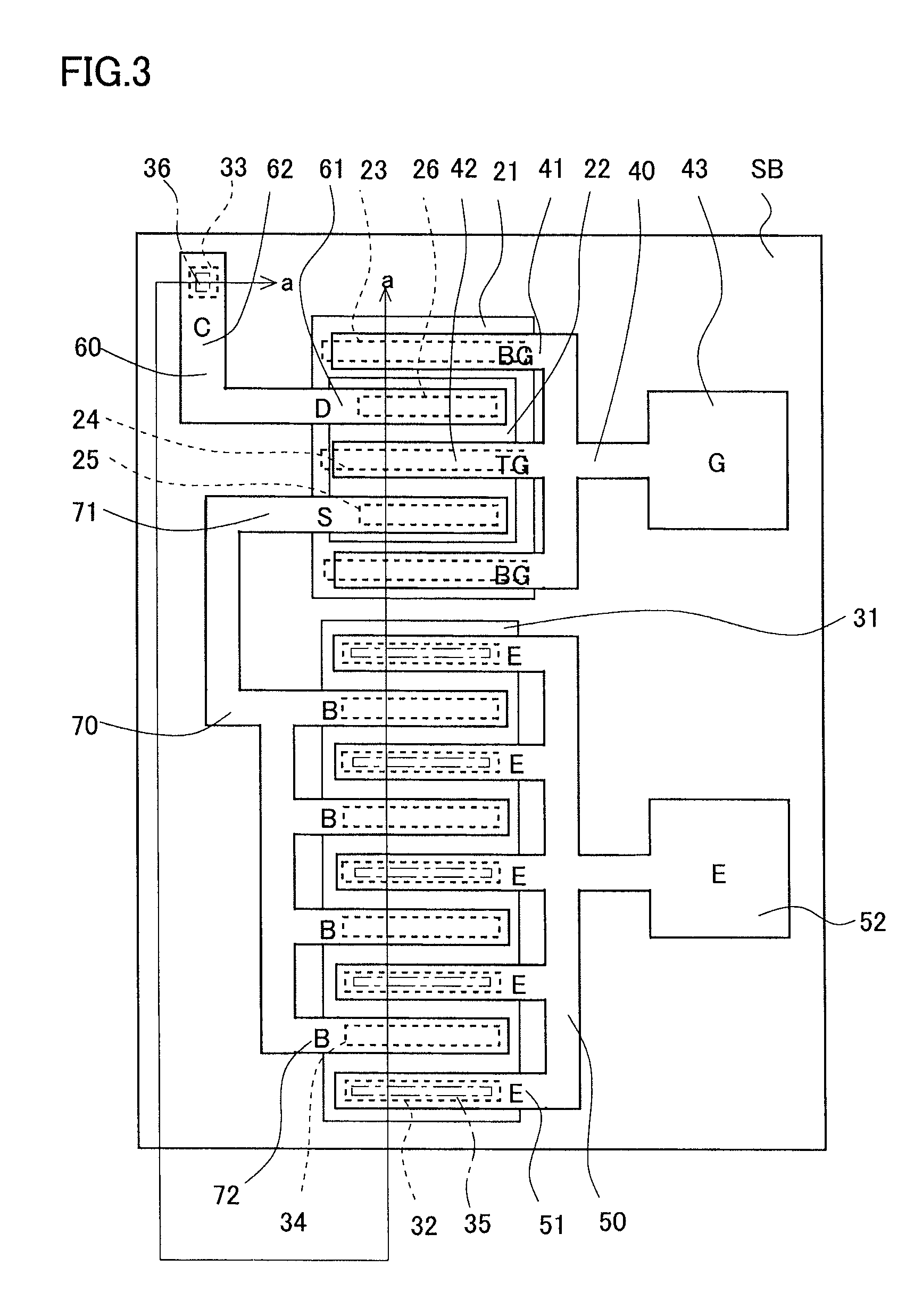
[0031]By referring to FIGS. 1 to 10, a preferred embodiment of the present invention will be described by taking, as an example, the case where an n channel type J-FET and an npn bipolar transistor are integrated on an n type semiconductor substrate.

[0032]FIG. 1 is a circuit diagram showing a connection example of an amplifying element 10 according to the preferred embodiment.

[0033]The amplifying element 10 is an element that is connected to an electret condenser microphone (ECM) 15 so as to perform impedance conversion and amplification. In the amplifying element 10, a junction field effect transistor (J-FET) 20 and a bipolar transistor 30 are integrated on a one conductivity type semiconductor substrate.

[0034]The ECM 15 has a vibration film (diaphragm) and an electrode facing thereto, which are arranged in a casing, and takes movements of the vibration film generated by sounds as changes in capacitance between the vibrating film and the electrode. The vibration film is configured ...


PUM


Abstract

An amplifier integrated circuit element or J-FET is used for impedance conversion and amplification of ECM. The amplifier integrated circuit element has advantages of allowing an appropriate gain to be set by adjusting a circuit constant, and of producing a higher gain than the J-FET; but also has a problem of having a complicated circuit configuration and requiring high costs. Using only the J-FET has also problems of outputting a voltage insufficiently amplified and producing a low gain. Against this background, provided is a discrete element in which: a J-FET and a bipolar transistor are integrated on one chip; a source region of the J-FET is connected to a base region of the bipolar transistor; and a drain region of the J-FET is connected to a collector region of the bipolar transistor. Accordingly, an ECM amplifying element with high input impedance and low output impedance can be achieved.

Description

[0001]This application claims priority from Japanese Patent Application Number JP2008-086638, filed on Mar. 28, 2008, the content of which is incorporated herein by reference in its entirety.BACKGROUND OF THE INVENTION[0002]1. Field of the Invention[0003]The present invention relates to an amplifying element and a manufacturing method thereof, and particularly to an amplifying element that is preferably used for an amplifying device and a manufacturing method thereof.[0004]2. Description of the Related Art[0005]In order to perform impedance conversion and amplification of an electret condenser microphone (hereinafter referred to as ECM), a junction field effect transistor (hereinafter referred to as J-FET) or an amplifier integrated circuit element is used, for example (see Japanese Patent Application Publications Nos. 2003-243944 and Hei 5-167358, for example).[0006]FIG. 11 is a circuit diagram showing a conventional ECM 115 and an amplifying element 110 to be connected thereto. On...

Claims


Application Information

Patent Timeline
Patent Type & Authority Patents(United States)
IPC IPC(8): H04R3/00
CPCH03F3/1855
Inventor ONODERA, EIO
Owner SEMICON COMPONENTS IND LLC
Why Eureka
Eureka Blog
Learn More