Relief circuit

a circuit and circuit technology, applied in the field of circuit arrangement, can solve the problems of additional switching losses in switching components, troublesome voltage overshoots due to forward recovery time of diodes, etc., and achieve the effect of reducing voltage overshoot and avoiding voltage overshoo

Inactive Publication Date: 2012-01-24
SIEMENS AG
View PDF17 Cites 0 Cited by
  • Summary
  • Abstract
  • Description
  • Claims
  • Application Information

AI Technical Summary

Benefits of technology

[0006]A circuit arrangement for limiting voltage overshoots due to the forward recovery time of a first diode which is switched alternately between reverse-biased (non-conducting) and forward-biased (conducting) by switching of a switching element is provided. In this case it is provided that the first diode is connected in series with a first capacitor, and a pre-charging circuit for the first capacitor is provided, said circuit charging the first capacitor while the first diode is switched to reverse bias. The pre-charging at the first capacitor and the voltage associated therewith causes the first diode to start conducting by said voltage value earlier. The voltage overshoot is therefore reduced. If said voltage value exceeds the voltage overshoot of the first diode, the voltage overshoot can be avoided completely.

Problems solved by technology

Voltage overshoots due to the forward recovery time for diodes are problematic in particular in the case of very fast switching operations.
A further possibility consists in slowing down the switching operations, although this entails other disadvantages, such as, for instance, additional switching losses in switching components.

Method used


Image

  • Relief circuit
  • Relief circuit
  • Relief circuit

Examples


Embodiment Construction

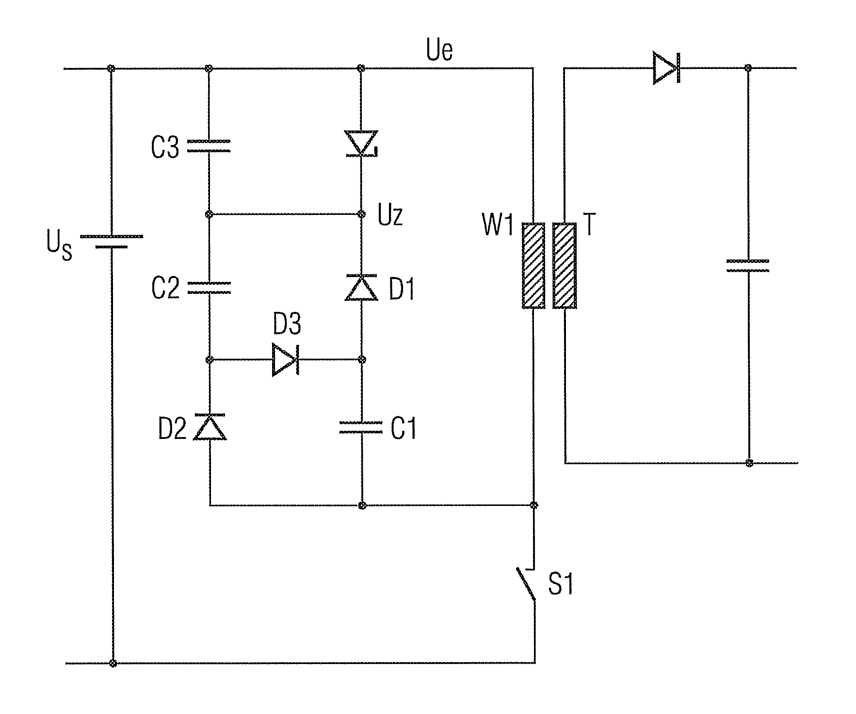
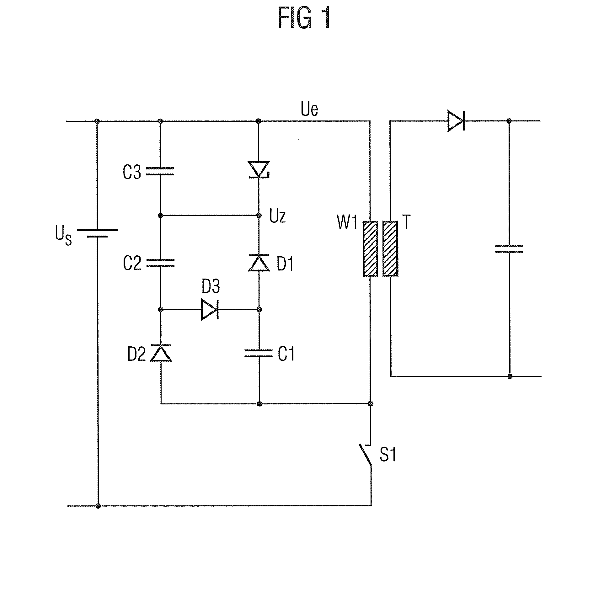
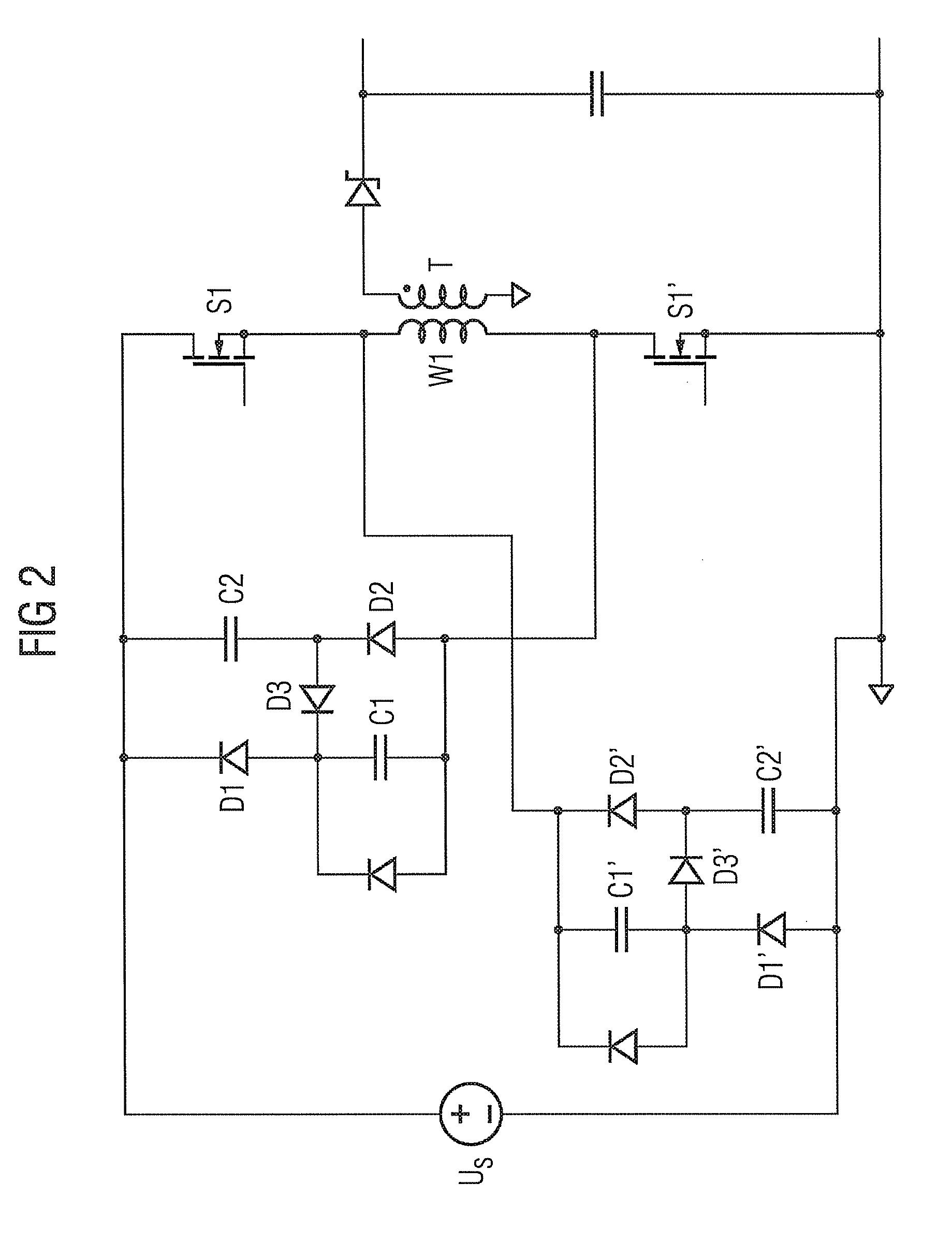
[0015]FIG. 1 shows a circuit arrangement having a switching element S1, which is typically a semiconductor switch, in particular a power switch. In the exemplary embodiment shown the switching element S1 is connected on the primary side of a transformer circuit in series with the primary winding W1 of a transformer T, and primary winding W1 and switching element S1 are connected to a direct-current voltage source US. By periodically opening and closing the switching element S1 the direct-current voltage of the direct-current voltage source US is converted into voltage pulses which are transferred via the transformer T onto the secondary side of the transformer circuit.

[0016]FIG. 1 also shows that a first diode D1 is connected in the circuit as a snubbing diode for the primary winding W1. The first diode D1 is switched to reverse-biased in relation to the direct-current voltage source US. If the switching element S1 is open, current flows via the intermediate circuit of the first dio...


PUM


Abstract

A circuit arrangement for limiting excessive voltages by a forward delay time of a first diode is described. The first diode is alternately switched in a non-conducting direction and a conducting direction by switching a circuit element. The first diode is series-connected to a first capacitor and a pre-charging circuit is provided for the first capacitor, the pre-charging circuit charging the first capacitor while the first diode is switched in the non-conducting direction. The pre-charging circuit charges the first capacitor more strongly than an excessive voltage of the first diode with regard to the amount.

Description

CROSS REFERENCE TO RELATED APPLICATIONS[0001]This application is the U.S. National Stage of International Application No. PCT / EP2007 / 063485 filed Dec. 7, 2007, and claims the benefit thereof. The International Application claims the benefits of Austrian Patent Application No. A 110 / 2007 AT filed Jan. 23, 2007; both of the applications are incorporated by reference herein in their entirety.FIELD OF INVENTION[0002]The invention relates to a circuit arrangement for limiting voltage overshoots due to the forward recovery time of a diode which is switched alternately between reverse-biased (non-conducting) and forward-biased (conducting) by switching of a switching element.BACKGROUND OF INVENTION[0003]Voltage overshoots due to the forward recovery time for diodes are problematic in particular in the case of very fast switching operations. With slow switching operations, the diode is usually made conducting by application of the forward bias voltage, which in the case of silicon diodes is...

Claims


Application Information

Patent Timeline
Patent Type & Authority Patents(United States)
IPC IPC(8): H02H7/122
CPCH02M1/34H02M3/335H02M3/3353H02M2001/346Y02B70/1491Y02B70/10H02M1/346
Inventor WEINMEIER, HARALD
Owner SIEMENS AG
Why Eureka
Try Eureka