
Method of forming a color filter touch sensing substrate

a technology of touch sensing and color filter, which is applied in the manufacture of electrode systems, instruments, electric discharge tubes/lamps, etc., can solve the problems of inability to thinne down the thickness of glass substrates b>36/b>, high cost, and low transmittance, so as to reduce the equivalent resistance of touch sensing structures/elements, increase the reliability of the display panel, and increase the sensitivity of the touch display panel

Active Publication Date: 2011-11-08
OPTRONIC SCI LLC
View PDF8 Cites 33 Cited by
  • Summary
  • Abstract
  • Description
  • Claims
  • Application Information

AI Technical Summary

Benefits of technology

"The present invention provides a method for integrating touch-sensing structures into a color filter touch sensing substrate, which increases the reliability of the display panel and allows for easier thinning of the panel. The method involves forming a transparent substrate, sequentially adding layers to the substrate, and patterning the layers to create the desired touch-sensing structures. The resulting color filter touch sensing substrate has improved reliability, increased variety of materials options, and easier manufacturing process."

Problems solved by technology

Therefore, the conventional touch display panel usually has problems such as heavyweight, high cost, large size, and low transmittance.
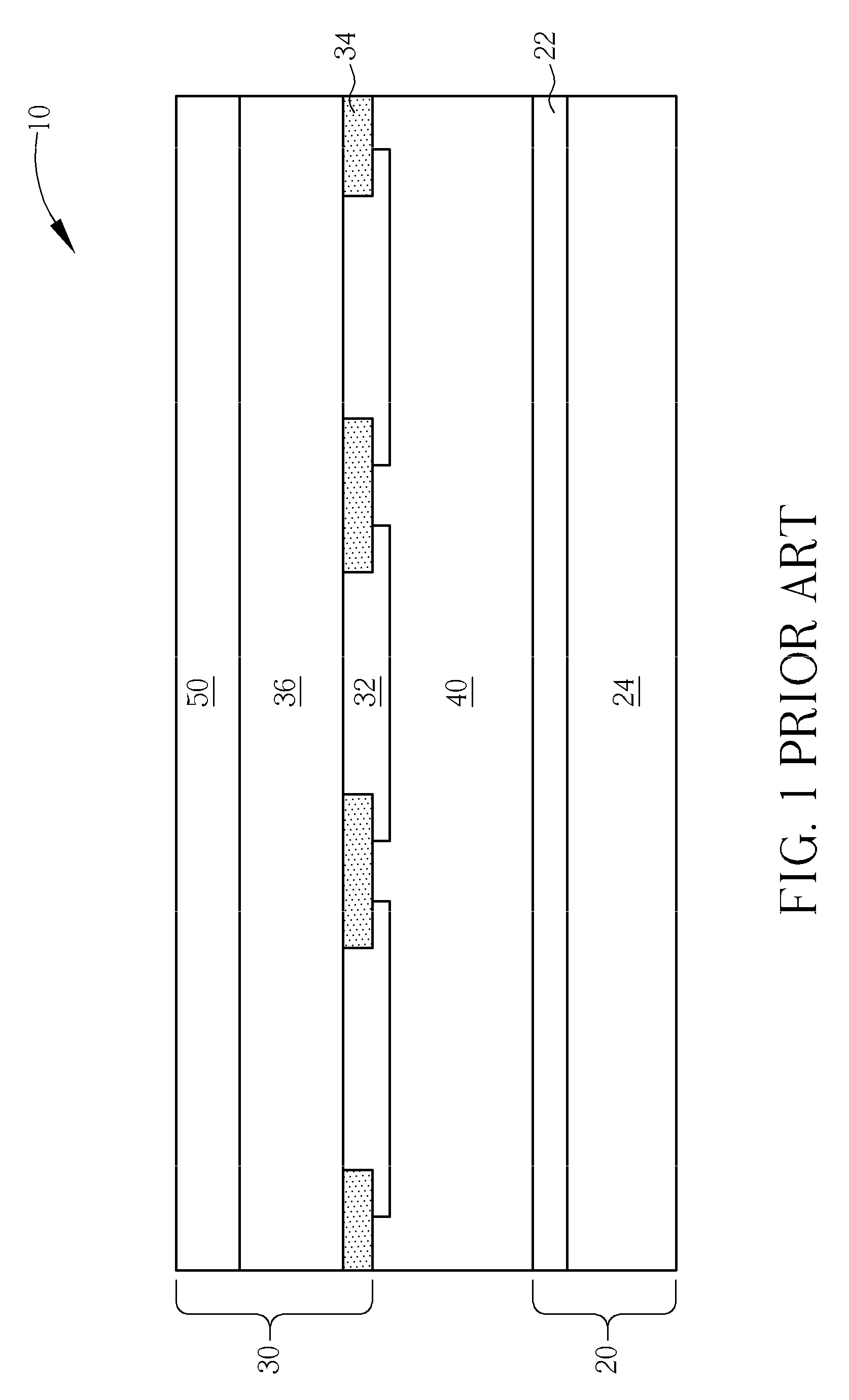
However, due to the fabricating method of the CF substrate 30, the thickness of the glass substrate 36 cannot be thinned down after the elements are formed on the two sides of the CF substrate 30.

Method used


Image

  • Method of forming a color filter touch sensing substrate
  • Method of forming a color filter touch sensing substrate
  • Method of forming a color filter touch sensing substrate

Examples


Embodiment Construction

[0021]To provide a better understanding of the presented invention, preferred embodiments will be detailed below. The preferred embodiments of the present invention are illustrated in the accompanying drawings with numbered elements.

[0022]FIG. 2 to FIG. 8 schematically illustrate a method of forming a color filter touch sensing substrate according to a first preferred embodiment of the present invention. FIG. 2 is an exploded diagram illustrating elements of the color filter touch sensing substrate. FIG. 3 to FIG. 7 are schematic top views illustrating the color filter touch sensing substrate. FIG. 8 is a schematic cross-sectional view illustrating the color filter touch sensing substrate 100 along a cross-section line A-A′ in FIG. 7. Like numbered numerals designate similar or the same parts, regions or elements. It is to be understood that the drawings are not drawn to scale and are only for illustration purposes. As shown in FIG. 2, a transparent substrate 102 is provided. The tr...


PUM

PropertyMeasurementUnit
thicknessaaaaaaaaaa
widthaaaaaaaaaa
thicknessaaaaaaaaaa

Abstract

A method of forming a color filter touch sensing substrate integrates touch-sensing structures / elements of a touch panel into the inner side of the color filter substrate, which faces a thin film transistor substrate, and forms patterned assistant electrodes on the surfaces of the transparent sensing pads for decreasing the equivalent resistance of the touch-sensing structures / elements. Moreover, since an adjacent transparent conductive layer and an assistant electrode layer are patterned to form the transparent sensing pads and the patterned assistant electrodes, a simplified pattern-transferring process can be applied to the transparent sensing pads and the patterned assistant electrodes, or bridge structures can be formed from the assistant electrode layer for electrically connecting between some transparent sensing pads. Therefore, the forming process is simplified.

Description

BACKGROUND OF THE INVENTION[0001]1. Field of the Invention[0002]The present invention is related to a method of forming a color filter touch sensing substrate, and more particularly, to a method of forming a color filter touch sensing substrate with capacitive touch function and capacitive structures (capacitive elements).[0003]2. Description of the Prior Art[0004]Since portable information products, such as PDAs, mobile phones, notebooks, and tablet PCs have become more and more prevalent in everyday life, touch panels have been broadly applied to these products as an input interface. The touch panel has become one of the most important components in tablet PCs with high requirements, because it integrates the input functions with the output functions in the same interface (display).[0005]The conventional method of fabricating a touch display panel includes forming the touch panel and the display panel individually, then assembling the touch panel and the display panel afterwards. ...

Claims


Application Information

Patent Timeline
Patent Type & Authority Patents(United States)
IPC IPC(8): G03F7/00
CPCG06F3/0412G06F3/0446G06F3/0443G06F2203/04111
Inventor CHIEN, YU-FENGHUANG, CHAU-SHIANGYANG, TUN-CHUNLEE, SEOK-LYUL
Owner OPTRONIC SCI LLC
Learn More