Display apparatus and manufacturing method therefor

a display apparatus and self-emitting technology, applied in the direction of discharge tube/lamp details, discharge tube luminescnet screens, organic semiconductor devices, etc., can solve the problems of deformation of the characteristic, loss of light-emitting function of the device, and loss of the thin and lightweight structure of the organic el device, so as to prevent the occurrence of cracks in the inorganic insulating film, improve the reliability of the display apparatus, and effectively protect against moisture and oxygen

Active Publication Date: 2009-05-12
UDC IRELAND
View PDF13 Cites 15 Cited by
  • Summary
  • Abstract
  • Description
  • Claims
  • Application Information

AI Technical Summary

Benefits of technology

[0014]According to the present embodiment, a substrate is formed on the inorganic insulating film for sealing the organic EL device, whereby the neutral axis when a bending stress is applied can be brought close to the inorganic insulating film, and thus, occurrence of cracks in the inorganic insulating film can be prevented, which allows the organic EL device to be effectively protected against moisture and oxygen. As a result, the reliability of the display apparatus can be improved.
[0015]In addition, on the top surface side of the organic EL device, an inorganic insulating film for sealing the organic EL device is formed with no organic insulating film being provided therebetween, whereby degradation of the organic EL device due to moisture and oxygen during the manufacturing process and after the manufacture thereof can be suppressed.
[0016]In addition, also on the lower side of the organic EL device, an inorganic insulating film for sealing the organic EL device is further formed, whereby degradation of the organic EL device due to moisture and oxygen during the manufacturing process and after the manufacture thereof can be further suppressed.
[0017]In addition, the series of film formation processes from the formation of the organic EL layer to the formation of the inorganic insulating film is carried out consecutively in a vacuum environment, and thus, the organic EL layer can be sealed by the inorganic insulating film without being exposed to moisture and oxygen in the atmosphere during manufacturing, which allows degradation of the characteristics of the organic EL device to be further suppressed.

Problems solved by technology

On the other hand, because of using organic matter, the organic EL device easily reacts with moisture, oxygen, and the like, which can result in degradation of the characteristics thereof.
In other words, when the organic EL layer reacts with moisture and oxygen in the air to cause corrosion and oxidation, the degraded portion becomes a non-light-emitting part (a dark spot), resulting in the light-emitting function of the device being lost.
However, in this method, the thickness and weight of the glass plate cancels the feature of thin and lightweight structure of the organic EL device.
However, as an inorganic film which is provided for the purpose of protection against the surrounding air, a material, such as a silicon oxide film, a silicon nitride film, a silicon nitride-oxide film, or the like, which is inferior in flexibility to the resin film, is generally used.
Therefore, when stresses are concentrated on this layer, a crack is generated in some cases.
For example, when the entire display apparatus including the substrate on which the organic EL device is formed is bent, stresses are most concentrated on the substrate surface, and thus, stresses are concentrated on the inorganic film which is located on the surface, resulting in a rupture.
Such a crack in the inorganic film causes the sealing function to be lost, resulting in the organic EL device being degraded.
In addition, the resin film provided in the layer under the inorganic film has a high moisture permeability and moisture-holding ability, as compared to the inorganic film, and thus, the resin film adjacent to the organic EL device may cause the organic EL device to be degraded.
However, with a structure in which plural resin films and plural of inorganic films are repeatedly laminated, the number of manufacturing processes is increased, and the manufacturing cost is increased.

Method used


Image

  • Display apparatus and manufacturing method therefor
  • Display apparatus and manufacturing method therefor
  • Display apparatus and manufacturing method therefor

Examples


first embodiment

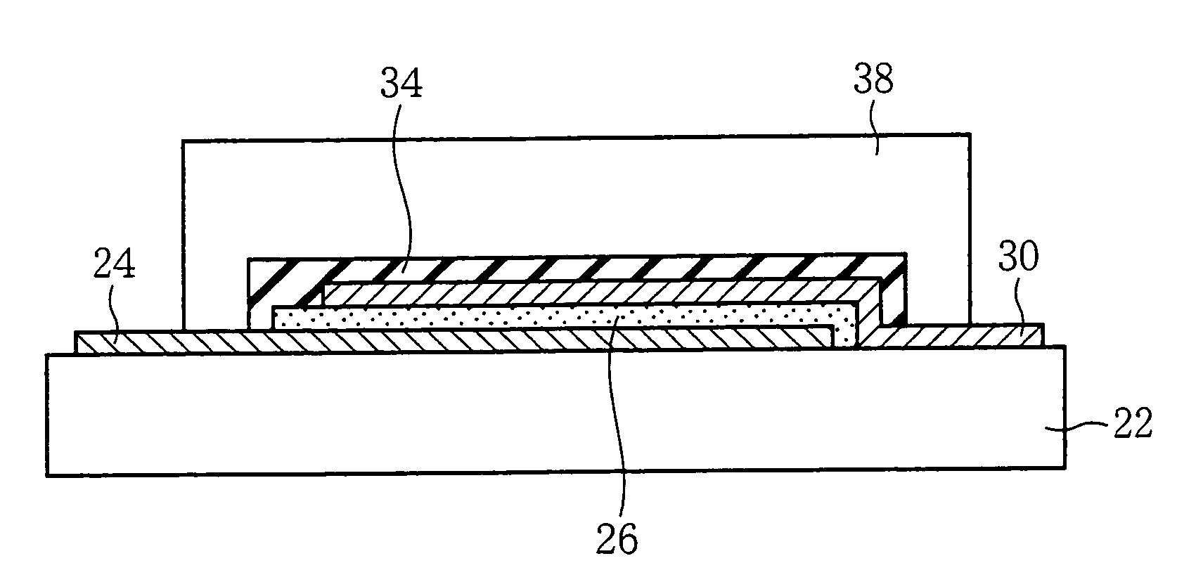
[0059]A display apparatus and a manufacturing method therefor according to a first embodiment of the present invention will be described with reference to FIGS. 3 to 5. FIG. 3 is a schematic sectional view illustrating the structure of the display apparatus according to the present embodiment, and FIGS. 4 and 5 are process sectional views illustrating the manufacturing method for a display apparatus according to the present embodiment.

[0060]First, the structure of the display apparatus according to the present embodiment will be described with reference to FIG. 3.

[0061]On a substrate 22 made up of polycarbonate, an electrode 24 of the anode side made up of ITO is formed. On the electrode 24, an organic EL layer 26 including a hole transport layer made up of α-NPD (diphenylnaphthyldiamine) and a luminescent layer made up of Alq3 (a quinolinol aluminum complex) is formed. On the organic EL layer 26, an electrode 30 of the cathode side made up of Al—Li is formed. Thereby, an organic EL...

second embodiment

[0083]A display apparatus and a manufacturing method therefor according to a second embodiment of the present invention will be described with reference to FIGS. 6 and 7. FIG.6 is a schematic sectional view illustrating the structure of the display apparatus according to the present embodiment, and FIG. 7 are process sectional views illustrating the manufacturing method for a display apparatus according to the present embodiment. The same components as those of the display apparatus according to the first embodiment and the manufacturing method therefor as shown in FIGS. 3 to 5 will be provided with the same signs, and the explanation thereof will be omitted or simplified.

[0084]First, the structure of the display apparatus according to the present embodiment will be described with reference to FIG. 6.

[0085]On a substrate 22 made up of polycarbonate, an electrode 24 of the anode side made up of ITO is formed. On the electrode 24, an organic EL layer 26 including a hole transport laye...

third embodiment

[0102]A display apparatus and a manufacturing method therefor according to a third embodiment of the present invention will be described with reference to FIGS. 8 and 9. FIG. 8 is a schematic sectional view illustrating the structure of the display apparatus according to the present embodiment, and FIG. 9 are process sectional views illustrating the manufacturing method for a display apparatus according to the present embodiment. The same components as those of the display apparatus according to the first and second embodiments and the manufacturing methods therefor as shown in FIGS. 3 to 7 will be provided with the same signs, and the explanation thereof will be omitted or simplified.

[0103]First, the structure of the display apparatus according to the present embodiment will be described with reference to FIG. 8.

[0104]On a substrate 22 made up of polycarbonate, an inorganic insulating film 40 made up of a silicon nitride-oxide film is formed. On the inorganic insulating film 40, an...


PUM


Abstract

A display apparatus including a substrate 22; an organic EL device including an electrode 24 which is formed on the substrate 22, an organic EL layer 26 which is formed on the electrode 24, and an electrode 30 which is formed on the organic EL layer 26; an inorganic insulating film 34 which is formed on the organic EL device, sealing the organic EL layer; and a substrate 38 which is formed on the inorganic insulating film 34, wherein the material and the thickness of the substrate 22 and the substrate 38 are set such that the neutral axis when a bending stress is applied is located in the vicinity of the interface between the inorganic insulating film 34 and the substrate 38. By configuring such a display apparatus, occurrence of cracks in the inorganic insulating film is prevented, and the organic EL device can be effectively protected against moisture and oxygen. As a result, the reliability of the display apparatus can be improved.

Description

TECHNICAL FIELD[0001]The present invention relates to a display apparatus and a manufacturing method therefor, and particularly relates to a self-emitting type display apparatus using an organic electroluminescent (EL) device and a manufacturing method therefor.BACKGROUND ART[0002]Conventionally, as a flat panel display, a liquid crystal display apparatus which uses a liquid crystal molecule as a shutter has been mainly used. In recent years, as a display apparatus which achieves further ultra-thinness and expanded display size, a self-emitting type display apparatus using an organic EL device has attracted attention.[0003]The display apparatus using an organic EL device has a structure in which plural devices including an electrode (anode) in the shape of a stripe that is made up of a transparent conductive film; an electrode (cathode) in the shape of a stripe that is made up of a metallic thin film, and is orthogonal to the anode; and an organic EL layer formed between these elect...

Claims


Application Information

Patent Timeline
Patent Type & Authority Patents(United States)
IPC IPC(8): H01J63/04H01J1/62H01L51/52H05B33/02H05B33/04H05B33/10H05B33/14H05B33/22
CPCH01L51/5237H01L2251/5338H01L2251/558H10K50/841H10K50/84H10K50/844H10K2102/311H10K2102/351
Inventor SAKAMOTO, YOSHIAKI
Owner UDC IRELAND
Why Eureka
Try Eureka