Solid-state imaging apparatus
a solid-state imaging and apparatus technology, applied in the field of solid-state imaging apparatus, can solve the problems of increasing the width between pixels, serious layout limitations of a/d converters b, etc., and achieve the effect of reducing the pitch of pixels
- Summary
- Abstract
- Description
- Claims
- Application Information
AI Technical Summary
Benefits of technology
Problems solved by technology
Method used
Image
Examples
first embodiment
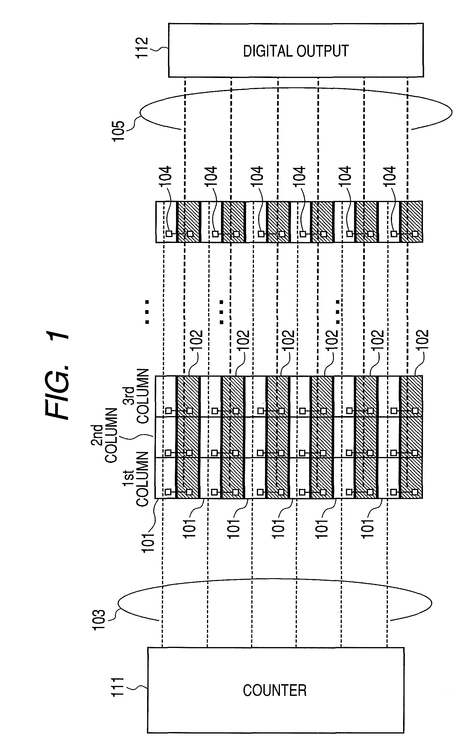
FIG. 2 is a diagram illustrating a configuration example of a solid-state imaging apparatus according to a first embodiment of the present invention. Pixels 106 are arranged in a two-dimensional array. The pixel 106 includes a photodiode, for example, and generates an image signal based on photoelectric conversion. Each of the pixels includes an amplifying unit which outputs a voltage signal based on an electric charge generated in the photodiode. A vertical scanning circuit 113 selects the pixels 106 by row unit, and reads out analog signals generated in the selected pixels 106 into A / D (analog / digital) converters 107 in a direction along a column. The A / D converter 107 is arranged at each of the columns of the pixels 106, and converts an analog signal into a digital signal. A counter 111 is arranged commonly to respective columns of the pixels 106 to count a digital signal value. First accumulation units 101, of which number is n, are arranged corresponding to each column of the p...
second embodiment
FIG. 3 is a diagram showing another configuration example of the region A of FIG. 2 according to a second embodiment of the present invention. The same components as in FIGS. 1 and 2 are shown by the same reference numerals and characters. Accumulation unit groups each made by the first accumulation unit 101 and the second accumulation unit 102 arranged adjacently in a direction along the row and paired, of which number is n, are arranged in the direction along the column.
The inter-accumulation unit wiring 104 is connected between the first accumulation unit 101 and the second accumulation unit 102 adjacent in the direction along the row. The data line 103 is connected to the first accumulation unit 101. The output line 105 is connected to the second accumulation unit 102. In the present embodiment, the pixel arrangement pitch in the direction along the row also can be easily reduced by arranging each of the accumulation unit groups arranged correspondingly to each pixel column with...
third embodiment
FIG. 4 is a diagram illustrating another configuration example of the region A of FIG. 2 according to a third embodiment of the present invention. The same components as those in FIGS. 1 and 2 are shown by the same reference numerals and characters.
An accumulation unit group 1 is provided, in which the first accumulation unit 101 and the second accumulation unit 102 are adjacently arranged in the direction along the column in the arrangement order of the first accumulation unit 101—the second accumulation unit 102 and are paired. An accumulation unit group 2 is provided, in which the first accumulation unit 101 and the second accumulation unit 102 are adjacently arranged in the direction along the column in the arrangement order of the second accumulation unit 102—the first accumulation unit 101. The accumulation unit group 1 and the accumulation unit group 2 are adjacently arranged repeatedly in the arrangement order of the accumulation unit group 1—the accumulation unit group 2, i...
PUM
 Abstract
Description
Claims
Application Information
 - R&D
- Intellectual Property
- Life Sciences
- Materials
- Tech Scout
- Unparalleled Data Quality
- Higher Quality Content
- 60% Fewer Hallucinations
Browse by: Latest US Patents, China's latest patents, Technical Efficacy Thesaurus, Application Domain, Technology Topic, Popular Technical Reports.
© 2025 PatSnap. All rights reserved.Legal|Privacy policy|Modern Slavery Act Transparency Statement|Sitemap|About US| Contact US: help@patsnap.com


