Dosimetry device for charged particle radiation
a charge particle and dosimetry technology, applied in the field of dosimetry devices, can solve the problems of increasing the number of anode electrodes, increasing the number of substrates and the cost, and the resolution of the dose distribution cannot be increased, so as to increase the number of substrates and the cost, and increase the resolution of the dose distribution.
- Summary
- Abstract
- Description
- Claims
- Application Information
AI Technical Summary
Benefits of technology
Problems solved by technology
Method used
Image
Examples
first embodiment
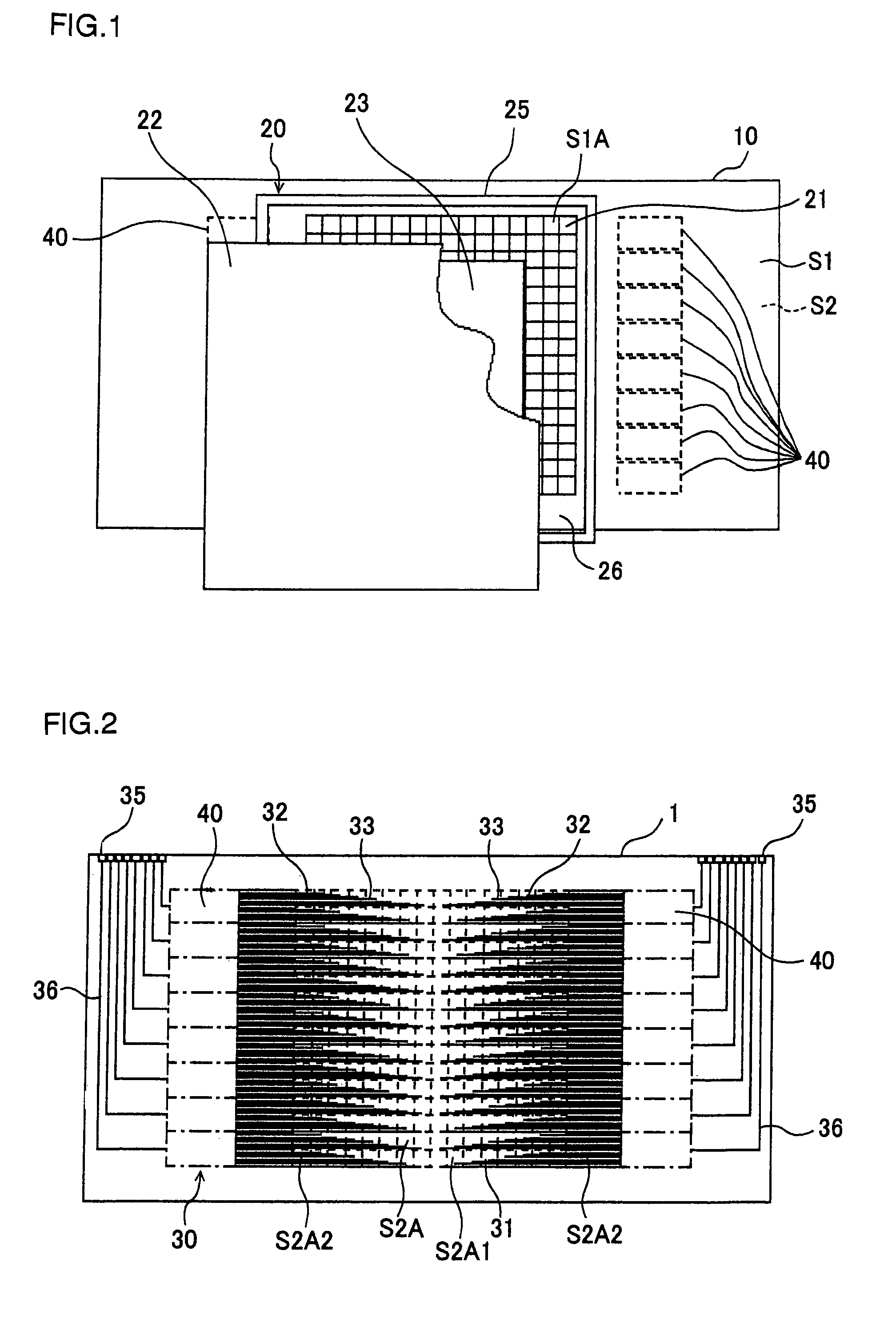
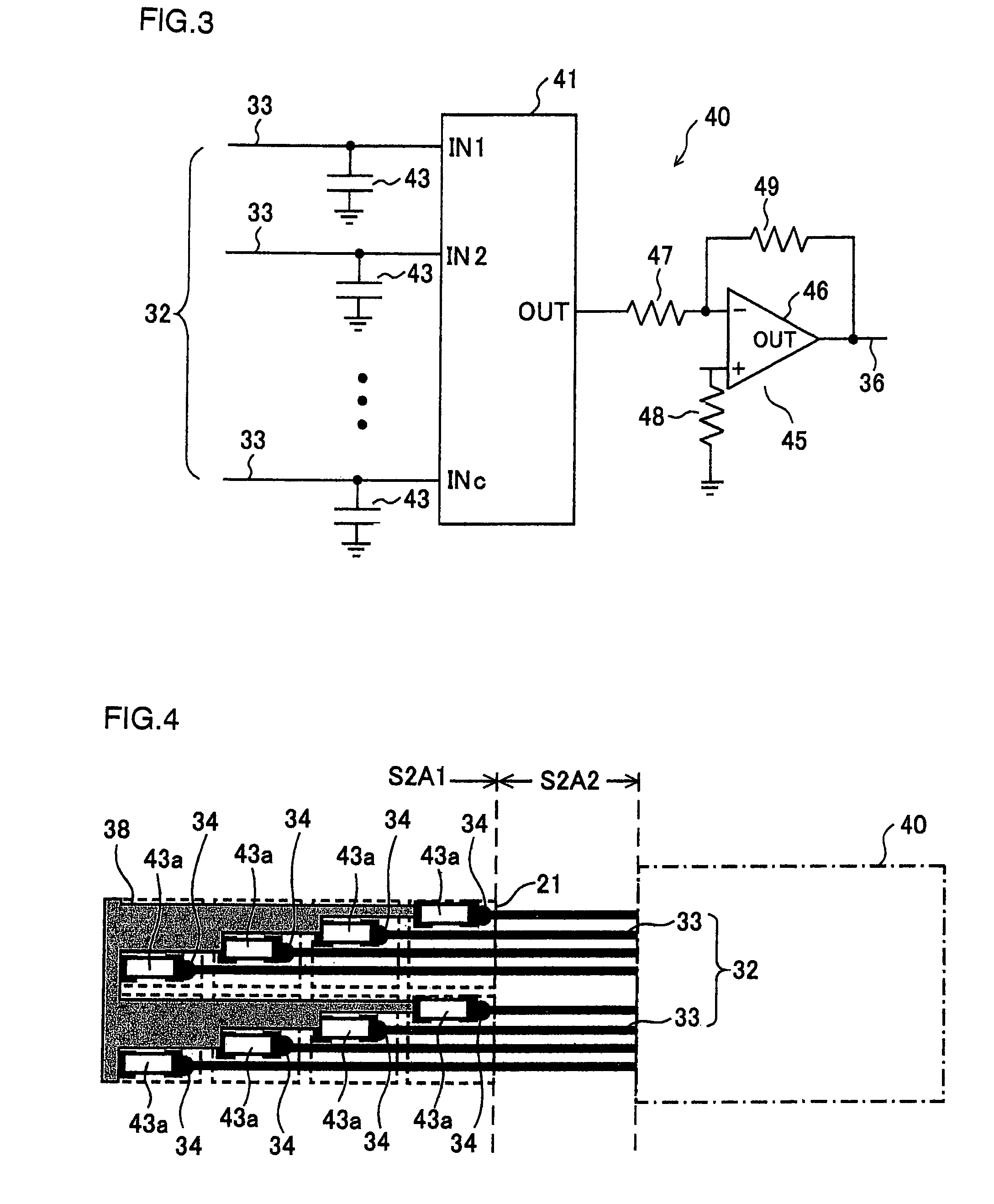
[0030]FIG. 1 is a view of a dosimetry device for charged particle radiation according to a first embodiment of the invention, FIG. 2 is a backside view of a printed circuit board according to the first embodiment, and FIG. 3 is an electrical circuit diagram of one signal processing block in a signal processing circuit according to the first embodiment.
[0031]With reference to FIG. 1, a single printed circuit board (PCB) 10 is used for the dosimetry device for charged particle radiation according to the first embodiment. The printed circuit board 10 has a pair of main surfaces S1 and S2 opposing to each other. The main surface S1 is for example a front surface of the printed circuit board 10, and the main surface S2 is the backside surface thereof. The printed circuit board 10 is a double-sided printed circuit board, and circuit elements are formed both on the main surfaces S1 and S2.
[0032]An ionization unit 20 is provided on the main surface S1 of the printed circuit board 10, and a ...
second embodiment
[0045]According to the first embodiment, the plurality of integrating capacitors 43 connected to the plurality of first electrodes 21 are provided in the second parts S2A2 unaffected by charged particle radiation in the central region S2A of the main surface S2. According to the second embodiment, the plurality of integrating capacitors 43 are ceramic capacitors 43a which are provided in the first part S2A1 of the central region S2A, in other words, at the backside surfaces of the first electrodes 21. The first part S2A1 has the plurality of first electrodes 21 therein, and the ceramic capacitors 43a are subjected to charged particle radiation. However, the ceramic capacitors 43a having high resistance against charged particle radiation can integrate and hold charge at the first electrodes 21 without the effect of the charged particle radiation though they are provided at the backside surfaces of the first electrodes 21.
[0046]FIG. 4 is a view showing the arrangement of one signal pr...
third embodiment
[0048]According to a third embodiment, the printed circuit board 10 according to the first embodiment is replaced by a multi-layer printed circuit board MPCB. The multi-layer printed circuit board MPCB includes number n of wiring layers 51, 52, 53, 54, . . . , 5(n −1), and 5n opposing and parallel to one another. A wiring layer positioned on the main surface S1 of the multi-layer printed circuit board MPCB is referred to as “first wiring layer 51” and a wiring layer positioned on the main surface S2 is referred to as “n-th wiring layer 5n.” A plurality of intermediate wiring layers other than the first and n-th wiring layers 51 and 5n are referred to as second wiring layer 52, third wiring layer 53, fourth wiring layer 54, . . . , and (n−1)-th wiring layer 5(n−1) sequentially from the first wiring layer 51 to the n-th wiring layer 5n.
[0049]An ionization unit 20 is provided on the main surface S1 of the multi-layer printed circuit board MPCB similarly to the first embodiment. More s...
PUM
 Abstract
Description
Claims
Application Information
 - R&D
- Intellectual Property
- Life Sciences
- Materials
- Tech Scout
- Unparalleled Data Quality
- Higher Quality Content
- 60% Fewer Hallucinations
Browse by: Latest US Patents, China's latest patents, Technical Efficacy Thesaurus, Application Domain, Technology Topic, Popular Technical Reports.
© 2025 PatSnap. All rights reserved.Legal|Privacy policy|Modern Slavery Act Transparency Statement|Sitemap|About US| Contact US: help@patsnap.com


