
Organic electroluminescence device and material for organic electroluminescence device

a technology of electroluminescence device and organic electroluminescence, which is applied in the direction of luminescnet screen of discharge tube, organic chemistry, natural mineral layered products, etc., can solve the problems of inability to reliably transfer energy to a phosphorescent host, inability to simply apply the fluorescent host to the host material, and inability to reliably transfer energy to a phosphorescent dopant. achieve the effect of less driving voltage, long life and high efficiency

Active Publication Date: 2011-10-18
IDEMITSU KOSAN CO LTD
View PDF59 Cites 13 Cited by
  • Summary
  • Abstract
  • Description
  • Claims
  • Application Information

AI Technical Summary

Benefits of technology

The invention provides a material for phosphorescent organic EL devices that can reduce driving voltage, exhibit high efficiency, and have a long lifetime. The material includes an organic-EL-device material represented by specific formulas, which, when used in an organic EL device, can lower the required driving voltage and increase efficiency and lifetime. The invention also provides an organic-EL-device material that can realize such an organic EL device. Overall, the invention provides a solution for creating more efficient and effective phosphorescent organic EL devices.

Problems solved by technology

Accordingly, it is not successful to simply apply the fluorescent host to the host material (phosphorescent host) for a phosphorescent-emitting layer.
Thus, energy cannot be reliably transferred to a phosphorescent dopant for emitting light having a wavelength in a visible light range of 520 nm to 720 nm.
Accordingly, an anthracene derivative is not suitable for the phosphorescent host.
Further, derivatives such as a perylene derivative, a pyrene derivative and a naphthacene derivative are not preferable phosphorescent hosts for the same reason above.
However, when applied with CBP as the host material, the organic EL device disclosed in the document 1 exhibits much higher luminous efficiency due to phosphorescent emission on one hand, but exhibits such a short lifetime as to be practically unusable on the other hand.
Such a problem is considered to be attributed to considerable degradation of molecules by holes due to not-high oxidation stability that the molecular structure of CBP exhibits.
Although the organic EL device disclosed in the document 2 exhibits improvement in the luminous efficiency and lifetime, the improved luminous efficiency and lifetime may not be always sufficient for practical application.
In the organic EL devices disclosed in the documents 10 to 14, which require relatively high driving voltage, lifetime of the devices may not be sufficiently prolonged.

Method used


Image

  • Organic electroluminescence device and material for organic electroluminescence device
  • Organic electroluminescence device and material for organic electroluminescence device
  • Organic electroluminescence device and material for organic electroluminescence device

Examples


synthesis example 1 (

Synthesis of Compound (A1))

[0303]

[0304]Under an argon gas atmosphere, 7.33 g (18 mmol) of bromide I-2, 6.70 g (18 mmol) of boronic acid I-1, 420 mg (0.36 mmol) of tetrakis(triphenylphosphine)palladium(0), 80 mL of toluene, 80 mL of dimethoxyethane and 26 mL of 2M sodium carbonate solution were added together, and stirred for 12 hours at 85 degrees C. Subsequently, the reaction mixture was cooled down to room temperature and added with water, and the aqueous phase was removed while the organic phase was condensed. Addition of nitrobenzene then followed, and the residue was thermally melted and subjected to filtration. Then, the residue was refined by silica-gel column chromatography and recrystallized by toluene, such that 6.48 g of the compound (A1) was obtained at an yield of 55%.

[0305]FD mass analysis consequently showed that m / e was equal to 654 while a calculated molecular weight was 654.

synthesis example 2 (

Synthesis of Compound (A3))

[0306]

[0307]Under an argon gas atmosphere, 7.33 g (18 mmol) of bromide I-2, 5.37 g (18 mmol) of boronic acid I-3, 420 mg (0.36 mmol) of tetrakis(triphenylphosphine)palladium(0), 80 mL of toluene, 80 mL of dimethoxyethane and 26 mL of 2M sodium carbonate solution were added together, and stirred for 12 hours at 85 degrees C. Subsequently, the reaction mixture was cooled down to room temperature and added with water, and the aqueous phase was removed while the organic phase was condensed. Addition of nitrobenzene then followed, and the residue was thermally melted and subjected to filtration. Then, the residue was refined by silica-gel column chromatography and recrystallized by toluene, such that 6.27 g of the compound (A3) was obtained at an yield of 60%.

[0308]FD mass analysis consequently showed that m / e was equal to 580 while a calculated molecular weight was 580.

synthesis example 3 (

Synthesis of Compound (A7))

[0309]

Under an argon gas atmosphere, 7.33 g (18 mmol) of bromide I-4, 5.37 g (18 mmol) of boronic acid I-3, 420 mg (0.36 mmol) of tetrakis(triphenylphosphine)palladium(0), 80 mL of toluene, 80 mL of dimethoxyethane and 26 mL of 2M sodium carbonate solution were added together, and stirred for 14 hours at 85 degrees C. Subsequently, the reaction mixture was cooled down to room temperature and added with water, and the aqueous phase was removed while the organic phase was condensed. Addition of nitrobenzene then followed, and the residue was thermally melted and subjected to filtration. Then, the residue was refined by silica-gel column chromatography and recrystallized three times by toluene, such that 5.02 g of the compound (A7) was obtained at an yield of 48%.

[0310]FD mass analysis consequently showed that m / e was equal to 580 while a calculated molecular weight was 580.


PUM

PropertyMeasurementUnit
triplet energyaaaaaaaaaa
wavelength of light emissionaaaaaaaaaa

Abstract

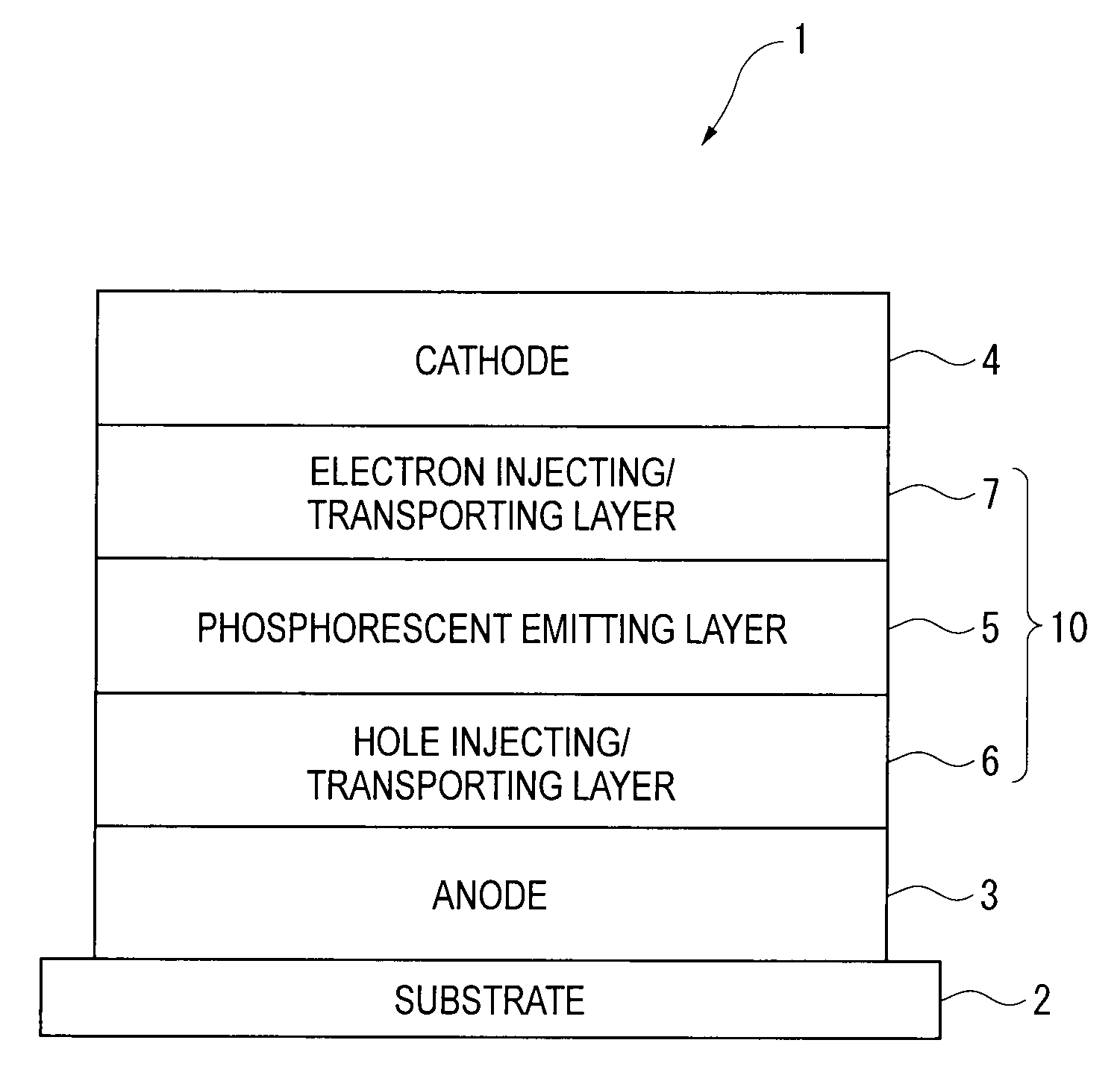
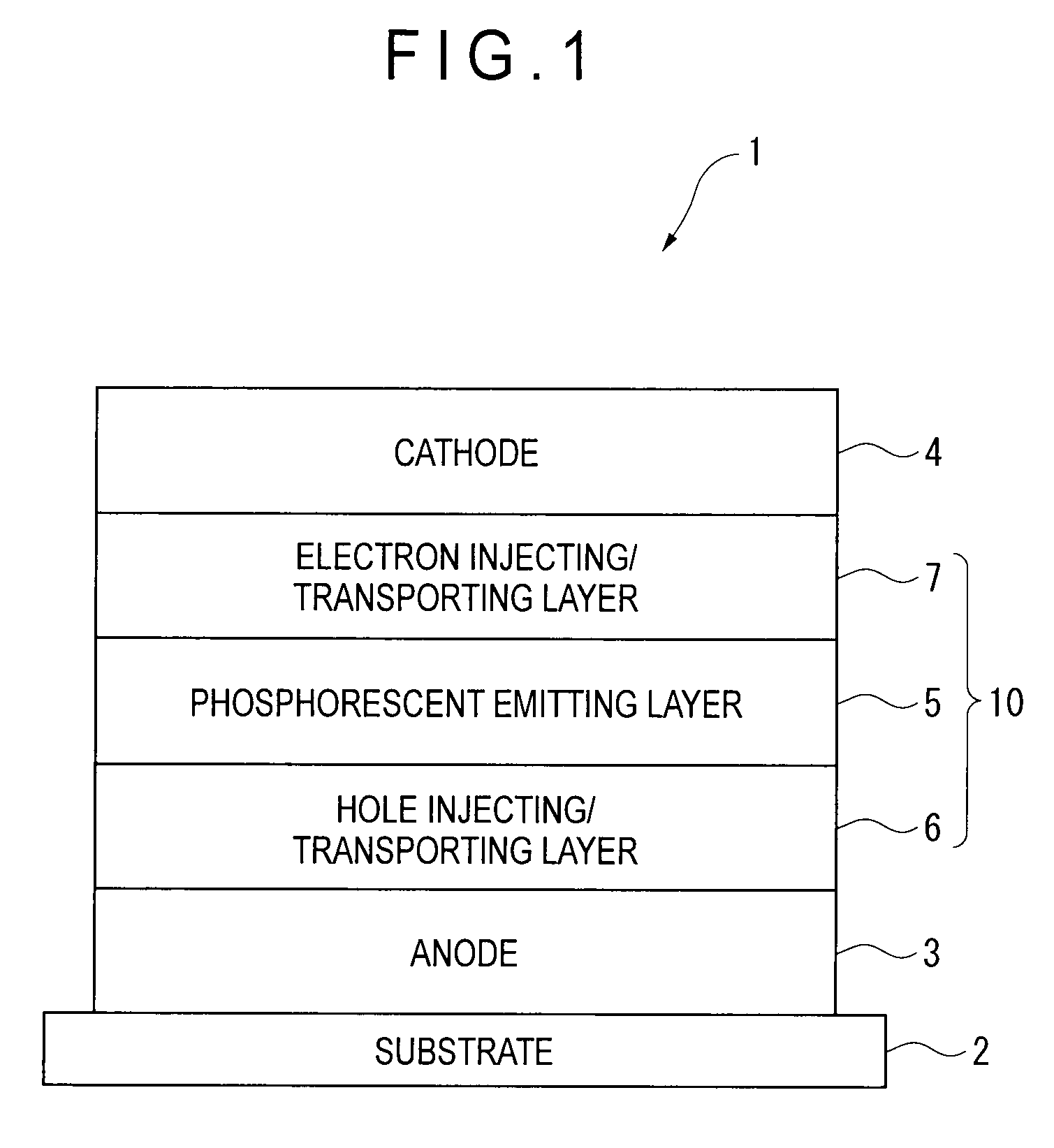
An organic electroluminescence device includes: a cathode; an anode; and a single-layered or multilayered organic thin-film layer provided between the cathode and the anode. In the organic electroluminescence device, at least one layer of the organic thin-film layer includes: an organic-electroluminescence-device material represented by a general formula selected from the following formulae (1), (2) and (3); and at least one phosphorescent material. In the formula: A represents a group selected from a 3-fluoranthenyl group, 5-benzo[c]phenanthrenyl group, 6-benzo[c]phenanthrenyl group and 10-benzo[g]chrysenyl group; Ar represents a fused aromatic ring having 10 to 30 carbon atoms and having triplet energy of 2.10 eV or more; and A or Ar is allowed to be substituted by a phenyl group or a naphthyl group.

Description

BACKGROUND OF THE INVENTION[0001]1. Field of the Invention[0002]The present invention relates to an organic electroluminescence device (hereinafter abbreviated as organic EL device as needed) and a material for the organic electroluminescence device. In particular, the present invention relates to an organic electroluminescence device including a red emitting layer and a material used for the organic electroluminescence device.[0003]2. Description of Related Art[0004]An organic EL device, which includes an organic thin-film layer (in which an emitting layer is included) between an anode and a cathode, has been known to emit light using exciton energy generated by a recombination of holes and electrons that have been injected into the emitting layer (e.g., see document 1: US2002 / 0182441, document 2: WO2005 / 112519, document 3: JP-A-2003-142267, document 4: WO2007 / 046658, document 5: JP-A-2006-151966, document 6: JP-A-2005-8588, document 7: JP-A-2005-19219, document 8: JP-A-2005-197262...

Claims


Application Information

Patent Timeline
Patent Type & Authority Patents(United States)
IPC IPC(8): H01L51/54H10K99/00
CPCC07C13/66C09K11/06C09K2211/1011C09K2211/185H05B33/14C07C2603/40C07C2603/42H10K85/626H10K85/633H10K85/324H10K85/342H10K50/11H10K2101/10H10K50/12
Inventor IWAKUMA, TOSHIHIROTAKASHIMA, YORIYUKIITO, MITSUNORIOGIWARA, TOSHINARI
Owner IDEMITSU KOSAN CO LTD
Learn More