
Impedance transformation with transistor circuits

a transistor circuit and transistor technology, applied in the field of impedance transformation with transistor circuits, can solve the problems of circuit arrangement, operating point consumption too much silicon area, and amplifier device can require very high input impedance,

Active Publication Date: 2011-08-23
INFINEON TECH AG
View PDF7 Cites 20 Cited by
  • Summary
  • Abstract
  • Description
  • Claims
  • Application Information

AI Technical Summary

Benefits of technology

The patent describes a method for creating a high impedance circuit at the input of an amplifier circuit using transistor circuits. This is achieved by using impedance transformations that involve differences in the channel width to channel length ratios of transistor circuits. The transistor circuits may have different overdrive voltages, which results in an exponential increase in impedance in relation to the difference in overdrive voltages. The method allows for control over the impedance value and can be implemented using NMOS and PMOS transistor circuits. The technical effect of the patent is to provide a high impedance circuit with good control over impedance value using transistor circuits.

Problems solved by technology

In some instances, an amplifier device can require very high input impedance.
Simply inserting a very large resistor between an input of the amplifier device and a bias point to generate an appropriate operating point consumes too much silicon area to be practical.
However, circuit arrangements relying on differing W / L ratios in a pair of transistor circuits for impedance transformation are only easily achievable for impedances in the mega-ohm range.
In order to produce impedances in the giga-ohm range for these circuit arrangements, currents on the order of picoamps may be required, making the impedance given by these circuit arrangements impractical.

Method used


Image

  • Impedance transformation with transistor circuits
  • Impedance transformation with transistor circuits
  • Impedance transformation with transistor circuits

Examples


Embodiment Construction

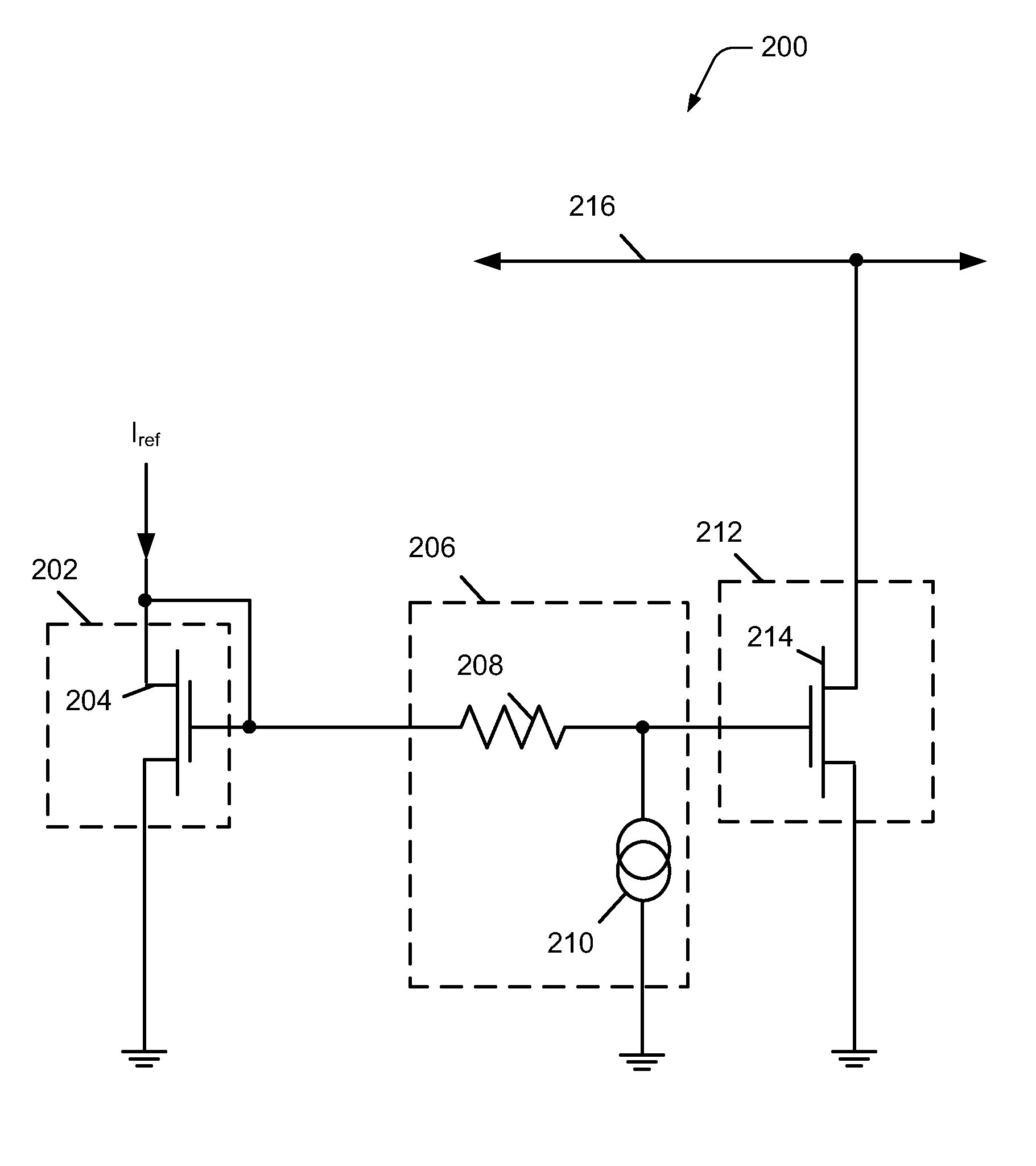
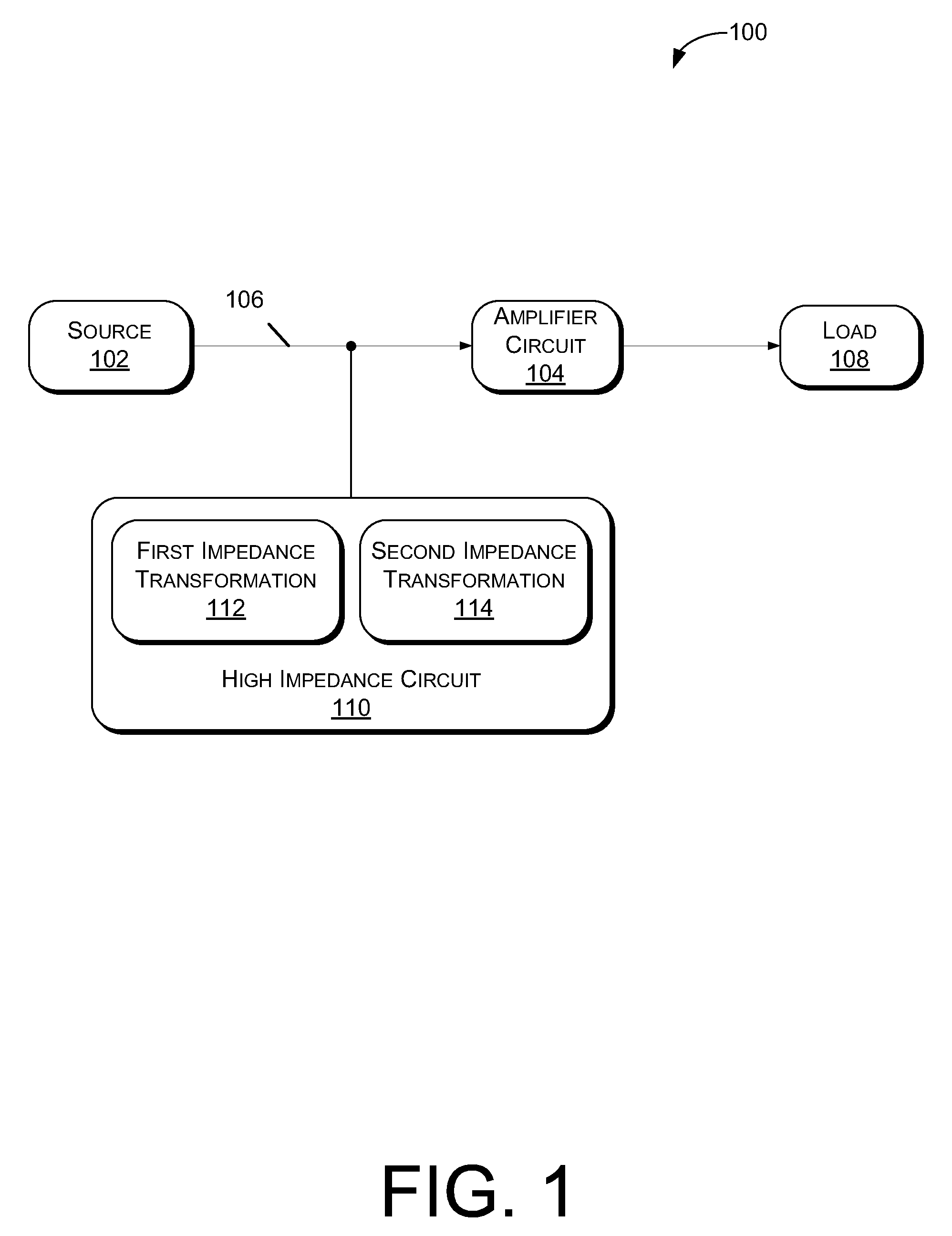
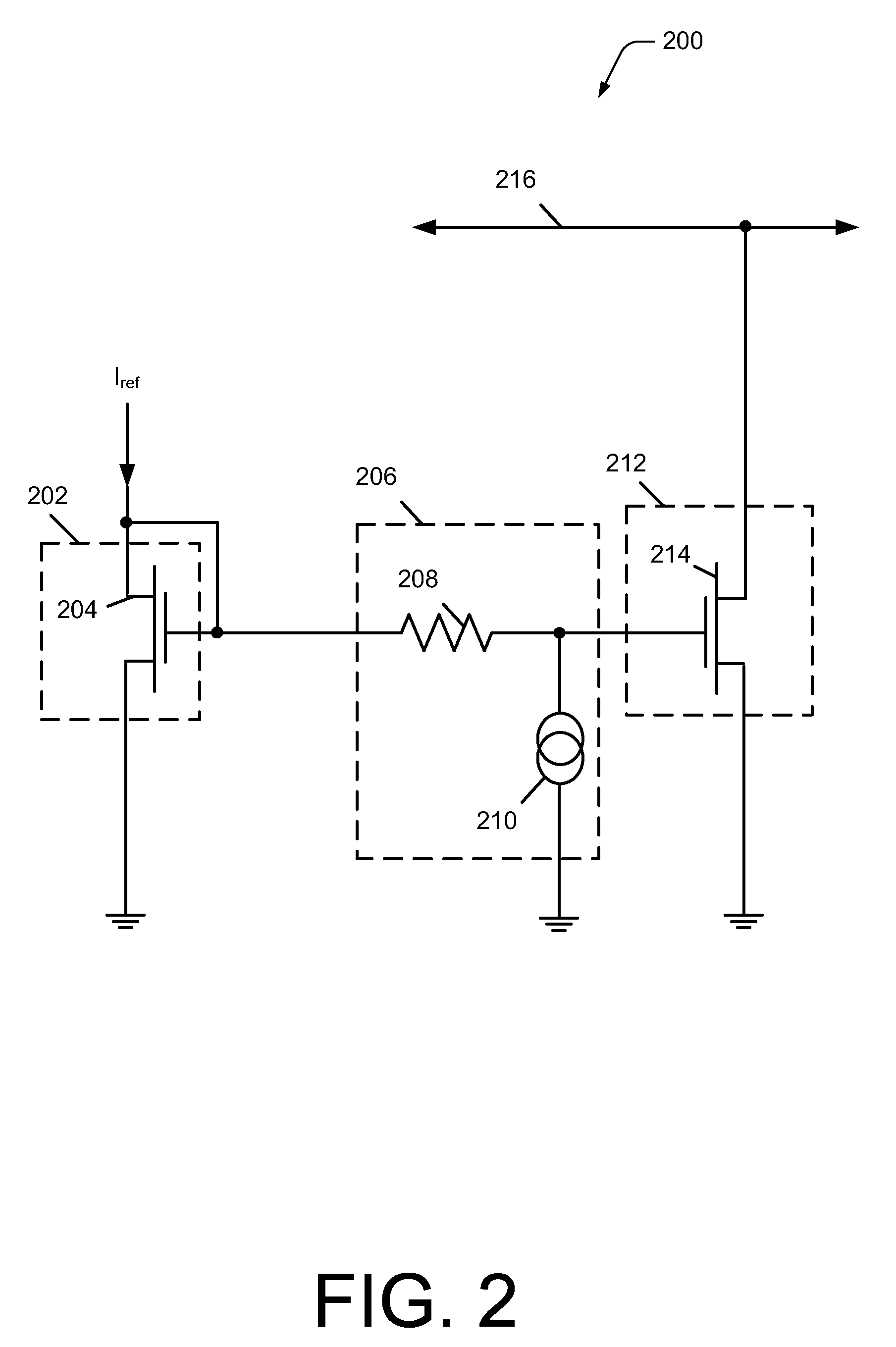
This disclosure describes using impedance transformations to provide a high impedance circuit at an input of an amplifier circuit using a relatively small amount of silicon area. In addition, the high impedance circuit utilizing the impedance transformations provides good control over the impedance value. The impedance transformations may be produced with negative channel metal oxide semiconductor (NMOS) transistor circuits and positive channel metal oxide semiconductor (PMOS) transistor circuits. Impedance transformation may take place due to differences in the channel width to channel length ratios of transistor circuit pairs.

Additionally, impedance transformation may take place due to differences in overdrive voltages of transistor circuit pairs. An overdrive voltage is defined by a gate-source voltage of a transistor circuit minus a threshold voltage of the transistor circuit. A transistor circuit having an overdrive voltage lower than the overdrive voltage of another transistor...


PUM


Abstract

An impedance transformation circuit utilizes two transistor circuits.

Description

BACKGROUNDIn some instances, an amplifier device can require very high input impedance. For example, a capacitive sensor feeding the amplifier device may require an impedance in the giga-ohm range. Simply inserting a very large resistor between an input of the amplifier device and a bias point to generate an appropriate operating point consumes too much silicon area to be practical.Impedance transformations may be used to increase input impedance of the amplifier circuit. One impedance transformation technique relates to coupling a pair of transistor circuits in a current mirror arrangement with each transistor circuit of the pair having a different channel width to channel length (W / L) ratio. In some implementations, the transistor circuit having a lower W / L ratio acts as an impedance device. In these implementations, the quotient in the W / L ratios of the transistor circuits is proportional to the impedance transformation. To illustrate, when the W / L ratio of a first transistor cir...

Claims


Application Information

Patent Timeline
Patent Type & Authority Patents(United States)
IPC IPC(8): G05F3/24G05F3/26
CPCG05F3/262H03F1/56G05F3/24H03F2200/222
Inventor DRAXELMAYR, DIETER
Owner INFINEON TECH AG
Learn More