
Optical near-field distribution transfer device

a transfer device and optical near-field technology, applied in the direction of optical elements, scanning probe techniques, instruments, etc., can solve the problems of limiting resolution, difficult to obtain a spatial resolution exceeding wavelength order by means of a usual microscopical technique, and nsom is not suitable for the use of transfer, etc., to achieve the effect of exceeding the limit of resolving power

Inactive Publication Date: 2011-06-07
RIKEN
View PDF4 Cites 0 Cited by
  • Summary
  • Abstract
  • Description
  • Claims
  • Application Information

AI Technical Summary

Benefits of technology

The device achieves long-distance transfer of super-resolution near-field images beyond the diffraction limit, improving image processing techniques and demonstrating the potential of metal nanostructures as dominant nanomaterials for nanoscale imaging and lithography.

Problems solved by technology

However, there is such a problem that the limit of resolution due to wave properties of light in imaging wherein a conventional light is used.
As described above, it is difficult to obtain a spatial resolution exceeding wavelength order by means of a usual microscopical technique.
Consequently, the NSOM is not suitable for the use of the transfer of such information and applying a parallel processing therefor.
Accordingly, there are such problems that restrictions for an operating frequency, a film thickness condition of the metal film and the like are extremely severe, so that there are many technical difficulties in the actual application of lithography and the like; and further that an out-of-focus image is unavoidable due to the loss of a metal.
However, such a problem that there are many technical difficulties in the actual application of lithography in also this manner has been pointed out.Non-patent literary document 1: S. Kawata et al. ed.

Method used


Image

  • Optical near-field distribution transfer device
  • Optical near-field distribution transfer device
  • Optical near-field distribution transfer device

Examples


Embodiment Construction

[0061]In the following, an example of embodiments of the optical near-field distribution transfer device according to the present invention will be described in detail by referring to the accompanying drawings.

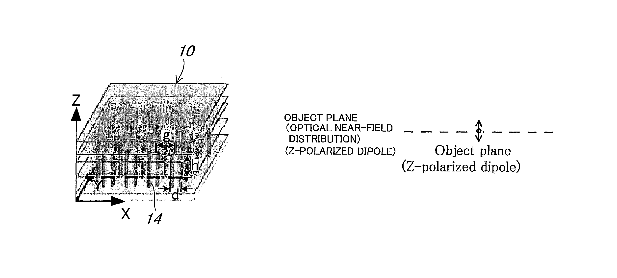
[0062]First, FIG. 3 is a conceptual, structural, perspective view for explaining a first embodiment of the optical near-field distribution transfer device according to the present invention.

[0063]An optical near-field distribution transfer device 10 is constituted in such that a plurality of, for example, columnar solid small rods 14 made of silver (Ag), each of which has a diameter d of a nanometer order (e.g. 20 nm) and a length h in the axial direction (a height along Z-direction) of a nanometer order (e.g. 50 nm) in the surrounding medium 12 such as a dielectric material, and a semiconductor having a dielectric constant ∈d is “∈d≧1”, are erected at predetermined spacing g (the spacing g corresponds to a distance within which an electric field emerging from a small rod 14 d...


PUM


Abstract

Long-distance transfer of a super-resolution near field can be performed with a wavelength condition of high degree of freedom. Not only an image in same size can be merely transferred, but also a magnified image can be transferred. Thus the processing technique of a near-field image is improved. Small rods are erected at predetermined spacing with one another on a two-dimensional plane. At least the exterior surface of each small rod is made of a predetermined material having a dielectric constant ∈m meeting the condition “∈m≦−∈d” where ∈d is the dielectric constant of the surrounding medium. The axes of the small rods can be extended to a predetermined direction with respect to the two-dimensional plane. An optical near-field is incidented to one end of each small rod.

Description

TECHNICAL FIELD[0001]The present invention relates to an optical near-field distribution transfer device, and particularly to an optical near-field distribution transfer device which is used suitably in case of imaging a material.BACKGROUND TECHNOLOGY[0002]Heretofore, it has been known that light propagates in the atmosphere, light can transmit material information in a wide spectrum extending from ultraviolet to infrared, and light is a probe capable of imaging a material even in the atmosphere or water which is different from an electron microscope, and an atom force microscope.[0003]It is recognized that such imaging by the use of light is an extremely important technology in also a field of bioscience or the like wherein an observation of, for example, a live cell in a subwavelength level is required.[0004]However, there is such a problem that the limit of resolution due to wave properties of light in imaging wherein a conventional light is used. Namely, the resolution of an ima...

Claims


Application Information

Patent Timeline
Patent Type & Authority Patents(United States)
IPC IPC(8): G02B27/10
CPCB82Y15/00B82Y20/00G02B6/1226G01Q60/22G02B5/008B82Y35/00
Inventor KAWATA, SATOSHIKATO, JUN-ICHIONO, ATSUSHI
Owner RIKEN
Learn More