
Voltage-controlled semiconductor structure, resistor, and manufacturing processes thereof

a voltage-controlled semiconductor and resistor technology, applied in the direction of semiconductor devices, diodes, electrical devices, etc., can solve the problems of large cost, large size of resultant resistors, and drawbacks of using additional masks and processes

Active Publication Date: 2011-03-22
SEMICON COMPONENTS IND LLC
View PDF5 Cites 4 Cited by
  • Summary
  • Abstract
  • Description
  • Claims
  • Application Information

AI Technical Summary

Benefits of technology

[0009]An object of this invention is to provide a semiconductor structure. The semiconductor structure comprises a substrate, a first doped well, and a second doped well. The substrate is doped with a first type of ions. The first doped well is with a second type of ions and is formed in the substrate. The second doped well is with the second type of ions and is formed in the substrate. The first type of ions and the second type of ions are complementary. A resistor is formed between the first doped well and the second doped well. A resistivity of the resistor relates to a first depth of the first doped well, a second depth of the second doped well, and a distance between the first doped well and the second doped well. The resistivity of the resistor is higher than that of a well resistor formed in a single doped well with the second type of ions.
[0010]Another object of this invention is to provide a voltage-controlled resistor. The voltage-controlled resistor comprises two ends respectively connected to two doped wells formed in a substrate. The substrate is with a first type of ions. The doped wells are with a complementary second type of ions. The two connecting ends connect to a high voltage and a low voltage respectively. The doped wells are split.
[0011]Another object of this invention is to provide a voltage-controlled resistor. The voltage-controlled resistor comprises two ends respectively connected to two doped wells formed in a substrate. The substrate is with a first type of ions. The doped wells are with a complementary second type of ions. The two connecting ends connect to a high voltage and a low voltage respectively. The doped wells are quasi-linked.
[0012]A further object of this invention is to provide a semiconductor process for forming a semiconductor resistor with high resistivity. The method comprises the steps of forming two deep wells in a substrate, wherein depletion regions respectively formed by the two doped wells and the substrate are connected, doping concentrations of the deep wells and the substrate are complementary; forming an oxide layer; forming a heavy-doped region in each of the deep wells; and forming two conducting ends connected the heavy-doped regions with conductive material.

Problems solved by technology

However, it has the drawbacks of using additional masks and processes, which costs a lot.
However, sizes of resultant resistors are still large.
Both of the two approaches have another common drawback, that is, both resistors cannot adjust the resistivity once the resistors are manufactured.
According to the aforementioned description, it is obvious that both current approaches have critical problems and limit the application of resistor in circuitry.

Method used


Image

  • Voltage-controlled semiconductor structure, resistor, and manufacturing processes thereof
  • Voltage-controlled semiconductor structure, resistor, and manufacturing processes thereof
  • Voltage-controlled semiconductor structure, resistor, and manufacturing processes thereof

Examples


first embodiment

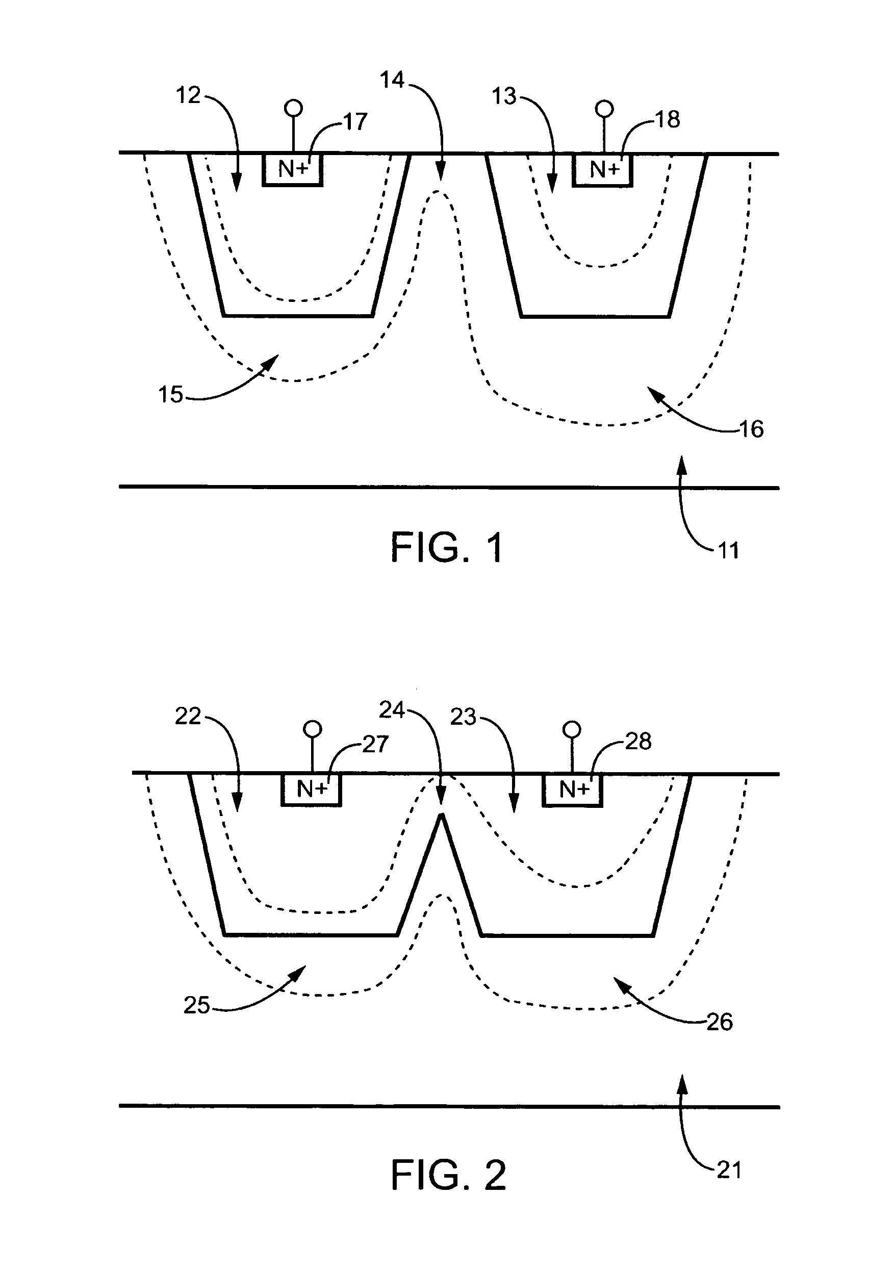
[0021]FIG. 1 illustrates the present invention, which is a voltage-controlled resistor. The resistor comprises a P-substrate 11 and two deep N-wells 12 and 13. There are two N+ regions 17 and 18 formed in the two deep N-wells 12 and 13 respectively as terminals of the resistor. The two deep N-wells 12 and 13 are formed in the P-substrate 11 and are split. An equivalent resistor 14 is formed between the two deep N-wells 12 and 13. The depletion region 15 is formed by the first deep N-well 12 and the P-substrate 11, and boundaries of the depletion region 15 are presented by two dashed lines. Similarly, the depletion region 16 is formed by the second deep N-well 13 and the P-substrate 11, and boundaries of the depletion region 15 are presented by two dashed lines. The two depletion regions 15 and 16 are connected.

[0022]A differential voltage is applied on the resistor via the N+ regions 17 and 18, causing a reverse bias between the P-type doped region, such as the P-substrate 11, and t...

second embodiment

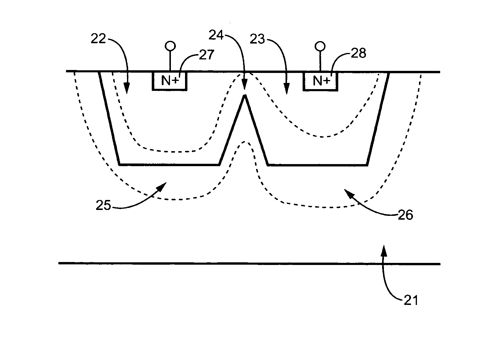
[0026]A differential voltage is applied on the resistor via the N+ regions 27 and 28, causing a reverse bias between the P-substrate 21, and the N-wells 22 and 23. The reverse bias affects the depletion region along with junction of the P-type doped region and the N-type doped region, and the differential thus controls electrical characters of the depletion region. In the second embodiment, a resistivity of the resistor is mainly determined by a resistivity of the equivalent resistor 24 and substantially increases after the differential voltage applied at the N+ regions 27 and 28 increases and results in pinch-off around the quasi-link region. When pinch-off occurs, connection of the N-wells 27 and 28 around the quasi-link region is interrupted by the depletion regions 25 and 26, and ions flowing through the equivalent resistor 24 dramatically decrease, which results in increase of the resistivity. The mechanism is controlled by the applied differential voltage, which achieves a vol...

fourth embodiment

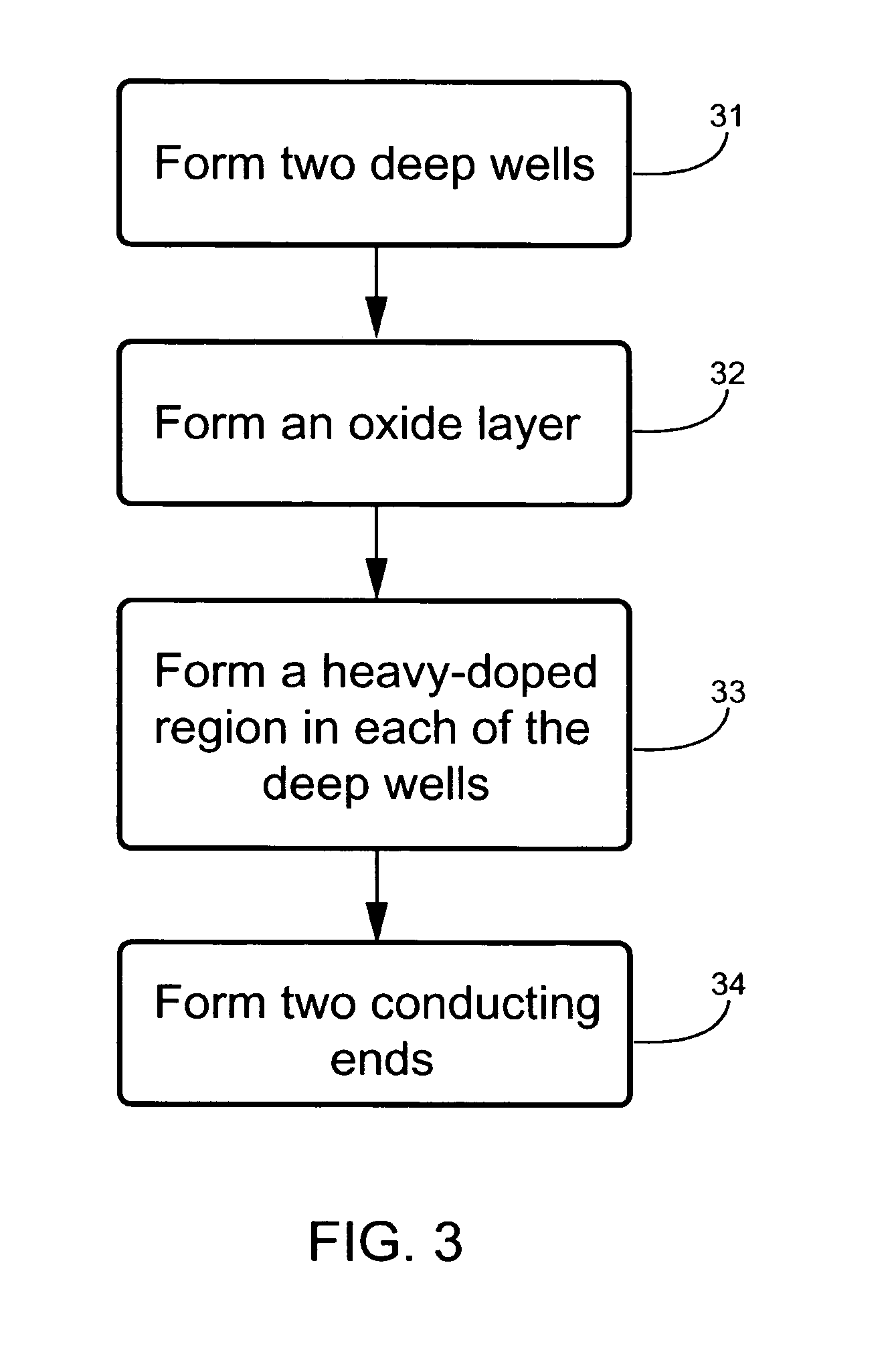
[0030]the present invention is a semiconductor process for forming a semiconductor resistor with high resistivity. The corresponding flowchart is illustrated in FIG. 3. First, step 31 is executed to form two deep wells in a substrate with complementary ions, wherein depletion regions respectively formed by the two doped wells and the substrate are connected. The step 31 further comprises thermal driving for 6 to 12 hours under 1000 to 1200 degrees of Celsius. Then, step 32 is executed to form an oxide layer. Step 33 is executed to form a heavy-doped region in each of the deep wells. Finally, step 34 is executed to form two conducting ends connected the heavy-doped regions with conductive material.

[0031]Alternatively, the heavy-doped region may be formed before the deep well being formed. That is, step 31 can be executed posterior to step 33. Moreover, the sequence of the aforementioned steps is for the purpose of an example. The sequence is not intended to be a limitation of the pre...


PUM


Abstract

Voltage-controlled semiconductor structures, voltage-controlled resistors, and manufacturing processes are provided. The semiconductor structure comprises a substrate, a first doped well, and a second doped well. The substrate is doped with a first type of ions. The first doped well is with a second type of ions and is formed in the substrate. The second doped well is with the second type of ions and is formed in the substrate. The first type of ions and the second type of ions are complementary. A resistor is formed between the first doped well and the second doped well. A resistivity of the resistor is controlled by a differential voltage. A resistivity of the resistor relates to a first depth of the first doped well, a second depth of the second doped well, and a distance between the first doped well and the second doped well. The resistivity of the resistor is higher than that of a well resistor formed in a single doped well with the second type of ions.

Description

CROSS-REFERENCES TO RELATED APPLICATIONS[0001]Not applicable.BACKGROUND OF THE INVENTION[0002]1. Field of the Invention[0003]The present invention relates to a voltage-controlled semiconductor structure, resistor, and manufacturing processes thereof; more particularly, relates to a voltage-controlled semiconductor structure and resistor with high resistivities and manufacturing process thereof.[0004]2. Descriptions of the Related Art[0005]Resistors with high resistivities are widely used in many electrical applications. Currently, there are two main approaches to manufacture resistors with high resistivities. The first approach is to use non-doped polysilicon as the resistor. The highest resistivity of this type of resistors is about 1K ohm / sq. The advantage of this approach is that sizes of resultant resistors are small. However, it has the drawbacks of using additional masks and processes, which costs a lot.[0006]The second approach is to manufacture a resistor with a lightly dope...

Claims


Application Information

Patent Timeline
Patent Type & Authority Patents(United States)
IPC IPC(8): H01L29/8605
CPCH01L29/66166H01L29/8605
Inventor CHIANG, CHIU-CHIHHUANG, CHIH-FENG
Owner SEMICON COMPONENTS IND LLC
Learn More