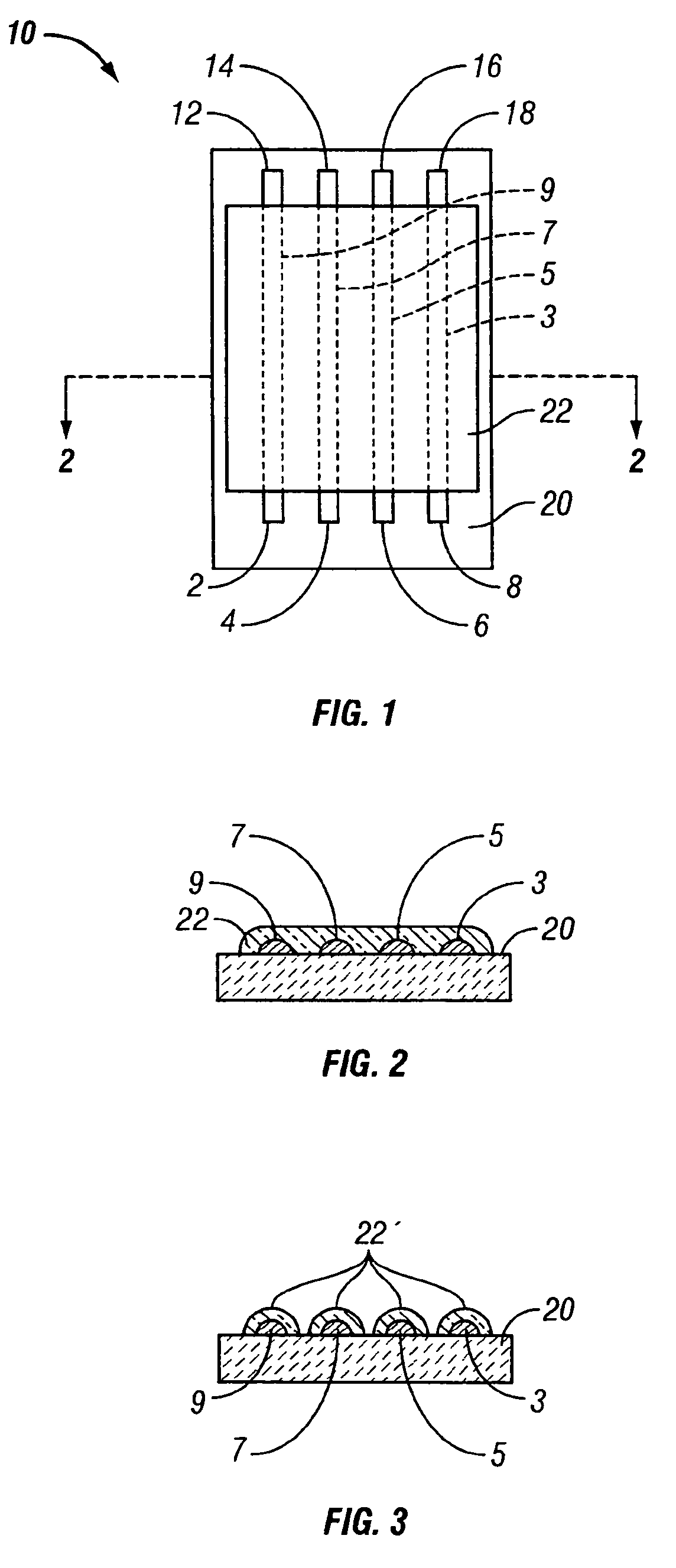
Hermetic implantable sensor
a sensor and implantable technology, applied in the field of hermetic implantable sensor, can solve the problems of complex structure, high manufacturing cost, and failures of electrodes and associated structures, and achieve the effect of minimizing failures and/or inaccuracy during implanted operation
- Summary
- Abstract
- Description
- Claims
- Application Information
AI Technical Summary
Benefits of technology
Problems solved by technology
Method used
Image
Examples
example 1
[0041]A pattern of Ferro 4082 Vitr-Au-Less high-purity platinum thick film paste is screen printed onto 96% alumina “multistrates.” The multistrates each contain nine 0.472-inch-diameter discs, each with 24 five-mil holes, previously formed by laser processing. The platinum paste is printed through a screen that was made with a “traces” pattern and a two-mil-thick emulsion. For each disc, the “traces” pattern consists of twenty-four approximately 10-mil-wide bands, one end of each of which overlaps one of the holes in the disc. A single layer of platinum thick film paste is printed in this pattern using two wet passes of the screen printer squeegee.
[0042]The platinum pattern is dried onto the multistrates in an oven at 150° C. for 20 minutes. The multistrates are then individually fired in air at peak temperatures of 1400, 1500, 1600, and 1700° C. for durations of either 10 or 60 minutes, resulting in eight different batches of nine discs each. Photographs of the discs are taken to ...
PUM
 Abstract
Description
Claims
Application Information
 - R&D
- Intellectual Property
- Life Sciences
- Materials
- Tech Scout
- Unparalleled Data Quality
- Higher Quality Content
- 60% Fewer Hallucinations
Browse by: Latest US Patents, China's latest patents, Technical Efficacy Thesaurus, Application Domain, Technology Topic, Popular Technical Reports.
© 2025 PatSnap. All rights reserved.Legal|Privacy policy|Modern Slavery Act Transparency Statement|Sitemap|About US| Contact US: help@patsnap.com


