Highly scalable thin film transistor

a thin film transistor, high-scalability technology, applied in the direction of basic electric elements, electrical appliances, semiconductor devices, etc., can solve the problems of shortening the channel and more unwanted dopant diffusion, and achieve the effect of minimizing dopant diffusion

Active Publication Date: 2011-02-15
SANDISK TECH LLC
View PDF33 Cites 95 Cited by
  • Summary
  • Abstract
  • Description
  • Claims
  • Application Information

AI Technical Summary

Benefits of technology

[0005]The present invention is defined by the following claims, and nothing in this section should be taken as a limitation on those claims. In general, the invention is directed to a FET having its channel region in polycrystalline semiconductor material, the FET formed by a method minimizing dopant diffusion.

Problems solved by technology

When the gate length of a field effect transistor (FET) is very small, there is danger that source and drain dopants will diffuse into the channel during high-temperature processing steps, potentially shorting the channel.
This problem is particularly acute when multiple stacked device levels are formed above a substrate in monolithic three dimensional memory arrays, as in Walker et al., U.S. Pat. No. 7,005,350, “Method for Fabricating Programmable Memory Array Structures Incorporating Series-Connected Transistor Strings.” In such a stacked array, each memory level may be subjected to repeated high-temperature steps, each causing more unwanted dopant diffusion.

Method used


Image

  • Highly scalable thin film transistor
  • Highly scalable thin film transistor
  • Highly scalable thin film transistor

Examples


first example

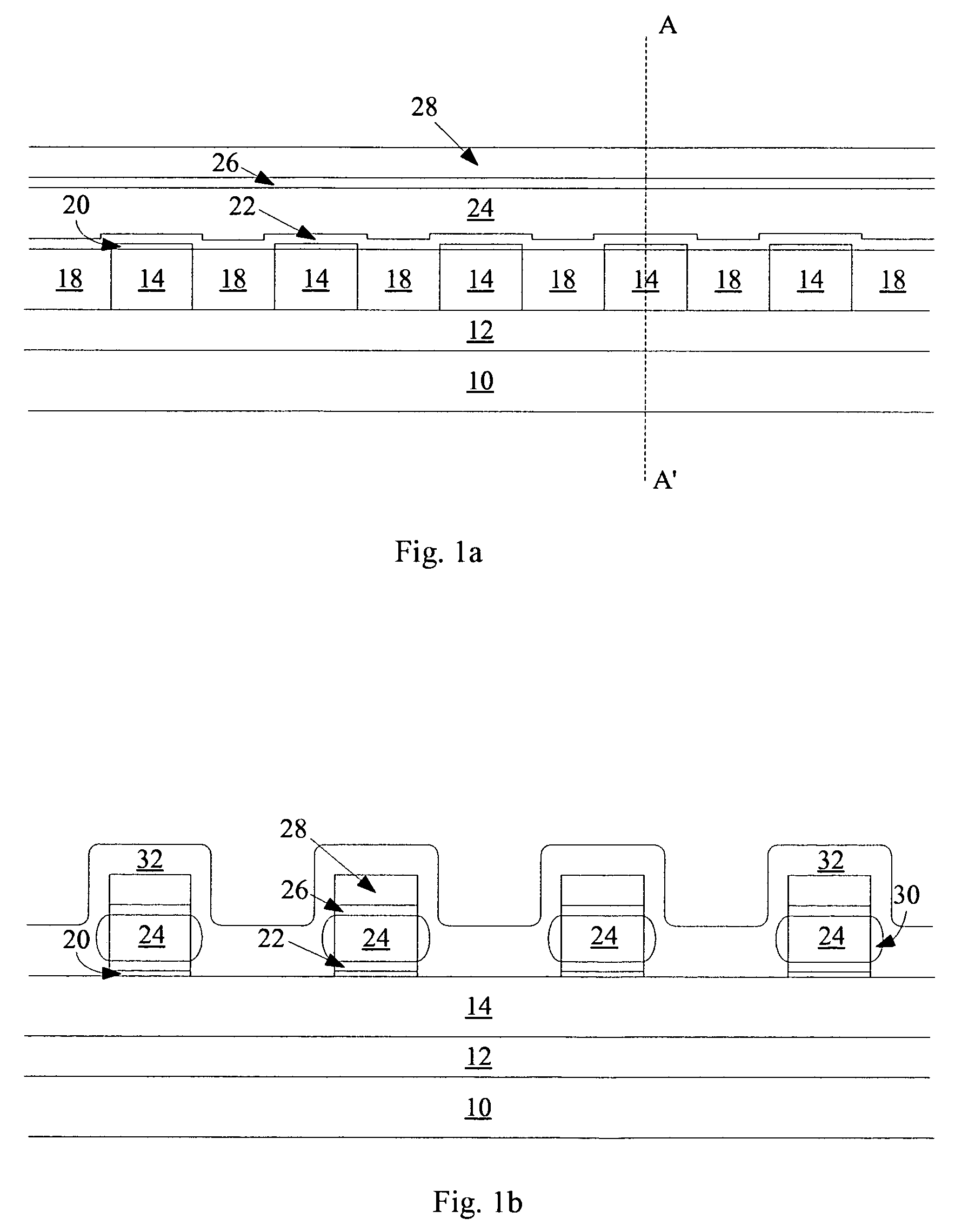
[0025]Fabrication begins on a suitable substrate. Turning to FIG. 1a, in some embodiments, substrate 10 may be a monocrystalline semiconductor substrate, for example a conventional silicon wafer. Control circuitry can be fabricated in the wafer substrate before fabrication of devices above the wafer begins. Alternatively, any other suitable substrate may be used, such as glass. Insulating layer 12 may be formed above substrate 10.

[0026]Channel layer 14 is deposited on insulating layer 12 by any conventional method, for example by chemical vapor deposition (CVD). Channel layer 14 is a semiconductor material, for example silicon, germanium, or silicon-germanium. In preferred embodiments, channel layer 14 is silicon-germanium, preferably between about 10 and about 40 atomic percent germanium, for example between about 10 and about 30 atomic percent germanium. In one embodiment, channel layer 14 is about 20 atomic percent germanium. Stated another way, channel layer 14 is SixGe1-x, wher...

second example

[0044]A second example will be provided of an embodiment of the present invention. In the second example, a charge storage element is formed between the channel region and the control gate, forming a charge storage memory cell.

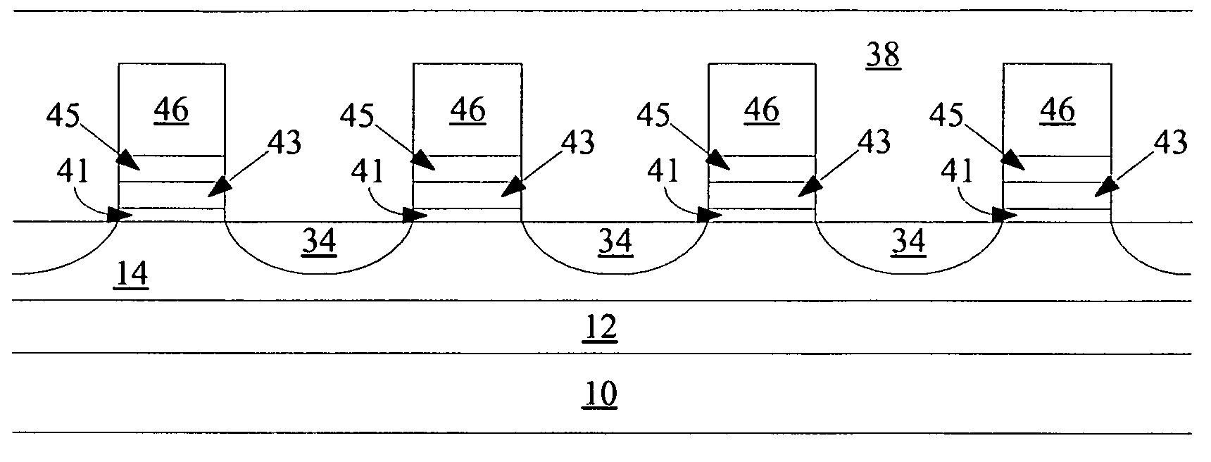
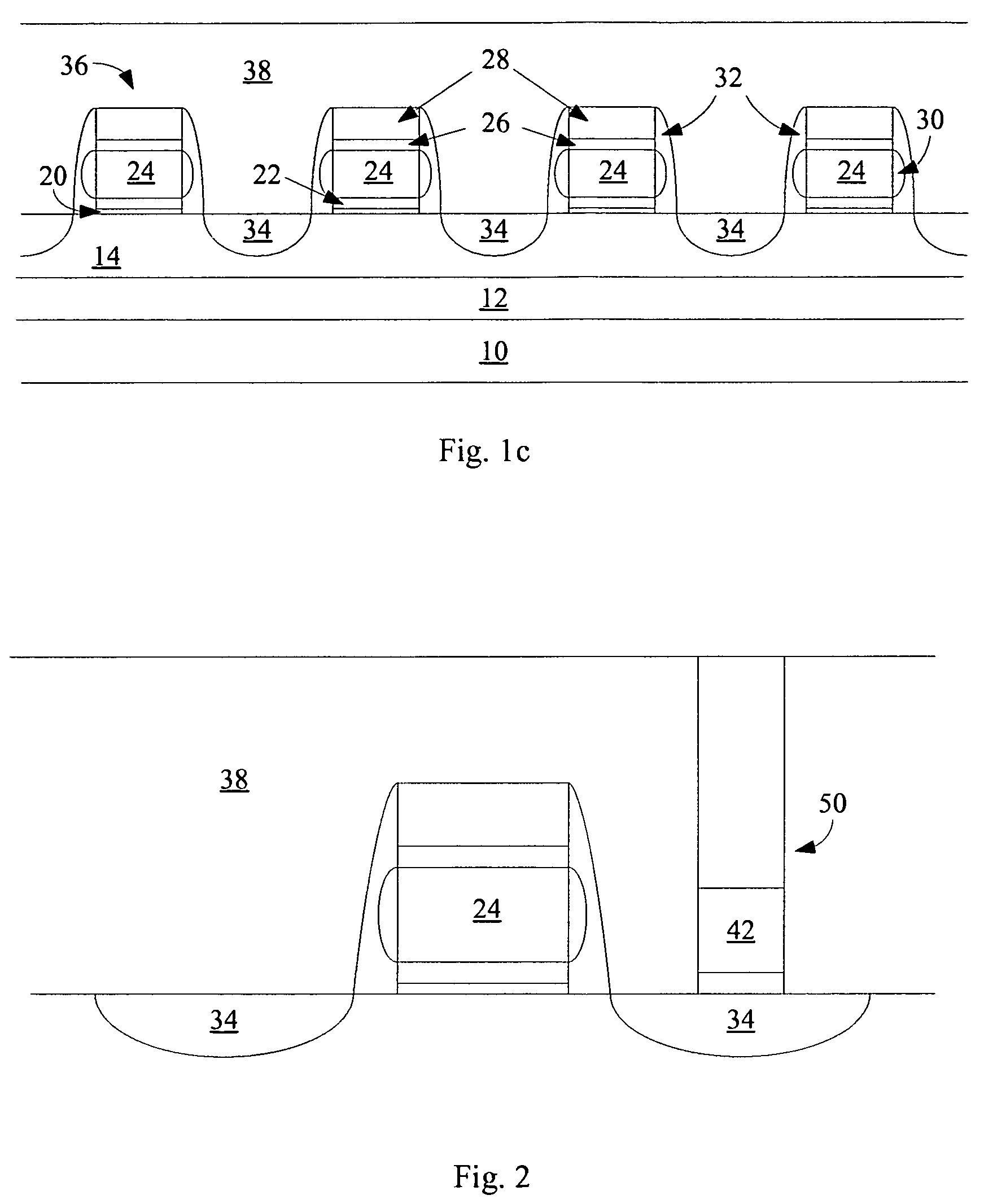
[0045]Turning to FIG. 3, fabrication begins as in the first example, with channel stripes 14 and dielectric material 18 formed above substrate 10 and dielectric 12, and exposed at a planar surface, for example by CMP. Channel stripes 14 may be formed of the same semiconductor materials named in the prior example, such as silicon-germanium. The view of FIG. 3 is in the same orientation as the view of FIG. 1b, viewing channel stripe 14 in cross-section extending left-to-right across the page.

[0046]Tunneling dielectric 41 is formed on this planar surface. This layer is preferably a thin, high-quality dielectric which will allow Fowler-Nordheim tunneling while the memory cell is being programmed and erased, but will prevent loss of charge in a programmed cell. In ...


PUM


Abstract

Shrinking the dimensions of PMOS or NMOS thin film transistors is limited by dopant diffusion. In these devices an undoped or lightly doped channel region is interposed between heavily doped source and drain regions. When the device is built with very short gate length, source and drain dopants will diffuse into the channel, potentially shorting it and ruining the device. A suite of innovations is described which may be used in various combinations to minimize dopant diffusion during fabrication of a PMOS or NMOS polycrystalline thin film transistor, resulting in a highly scalable thin film transistor. This transistor is particularly suitable for use in a monolithic three dimensional array of stacked device levels.

Description

RELATED APPLICATIONS[0001]This application is a divisional of U.S. application Ser. No. 11 / 765,269, filed Jun. 19, 2007 which is hereby incorporated by reference in its entirety.BACKGROUND OF THE INVENTION[0002]A field effect transistor (FET) has an undoped or very lightly doped channel region disposed between heavily doped source and drain regions. When the gate length of a field effect transistor (FET) is very small, there is danger that source and drain dopants will diffuse into the channel during high-temperature processing steps, potentially shorting the channel.[0003]This problem is particularly acute when multiple stacked device levels are formed above a substrate in monolithic three dimensional memory arrays, as in Walker et al., U.S. Pat. No. 7,005,350, “Method for Fabricating Programmable Memory Array Structures Incorporating Series-Connected Transistor Strings.” In such a stacked array, each memory level may be subjected to repeated high-temperature steps, each causing mo...

Claims


Application Information

Patent Timeline
Patent Type & Authority Patents(United States)
IPC IPC(8): H01L21/336
CPCH01L27/115H01L27/11568H01L27/11578H10B63/30H10B69/00H10B43/30H10B43/20
Inventor HERNER, S. BRADBANDYOPADHYAY, ABHIJIT
Owner SANDISK TECH LLC
Why Eureka
Try Eureka