Method and systems for advanced reprogrammable boot codes and in-application programming of embedded microprocessor systems
a microprocessor and embedded technology, applied in the field of advanced reprogrammable boot codes and in-application programming of embedded microprocessor systems, can solve the problems of long development cycle and its associated cost to achieve fully tested and verified software or firmware for boot codes, restricting the flexibility to make field, and limiting the speed of accessing memory in the boot-up process
- Summary
- Abstract
- Description
- Claims
- Application Information
AI Technical Summary
Benefits of technology
Problems solved by technology
Method used
Image
Examples
case 1
te 16 KB above address space (at 0x00—4000˜0x1F_FFFF) of Flash memory 702:
[0068]Step 1: Software first writes PWE bit=1 in PCON SFR register, to enable program write in CPU.
[0069]Step 2: Software writes FARM bit=1 in CSREPR SFR register, to enable Flash memory address re-mapping mechanism.
[0070]Step 3: Programming sequence for enabling “Byte Program” command for on-Flash memory:[0071]1. Write (0x4000+0x555)=0xAA[0072]2. Write (0x4000+0x2AA)=0x55[0073]3. Write (0x4000+0x555)=0xA0
[0074]Step 4: Software writes FARM bit=0, to disable Flash memory address re-mapping mechanism.
[0075]Step 5: Now perform the actual byte write command.[0076]1. Write PA=PD (where PA: any 16 KB above Flash memory address to be programmed, PD: write data)[0077]2. Repeatedly read PA. If equal to PD, then the Program command is completed.
[0078]Step 6: Software writes PWE bit=0, to disable program write in CPU.
case 2
d the lower 16 KB (at 0x00—0000˜0x00—3FFF) of Flash memory 702:
[0079]Step 1: Software first writes FARM bit=1 in CSREPR SFR register, to enable Flash memory address re-mapping mechanism.
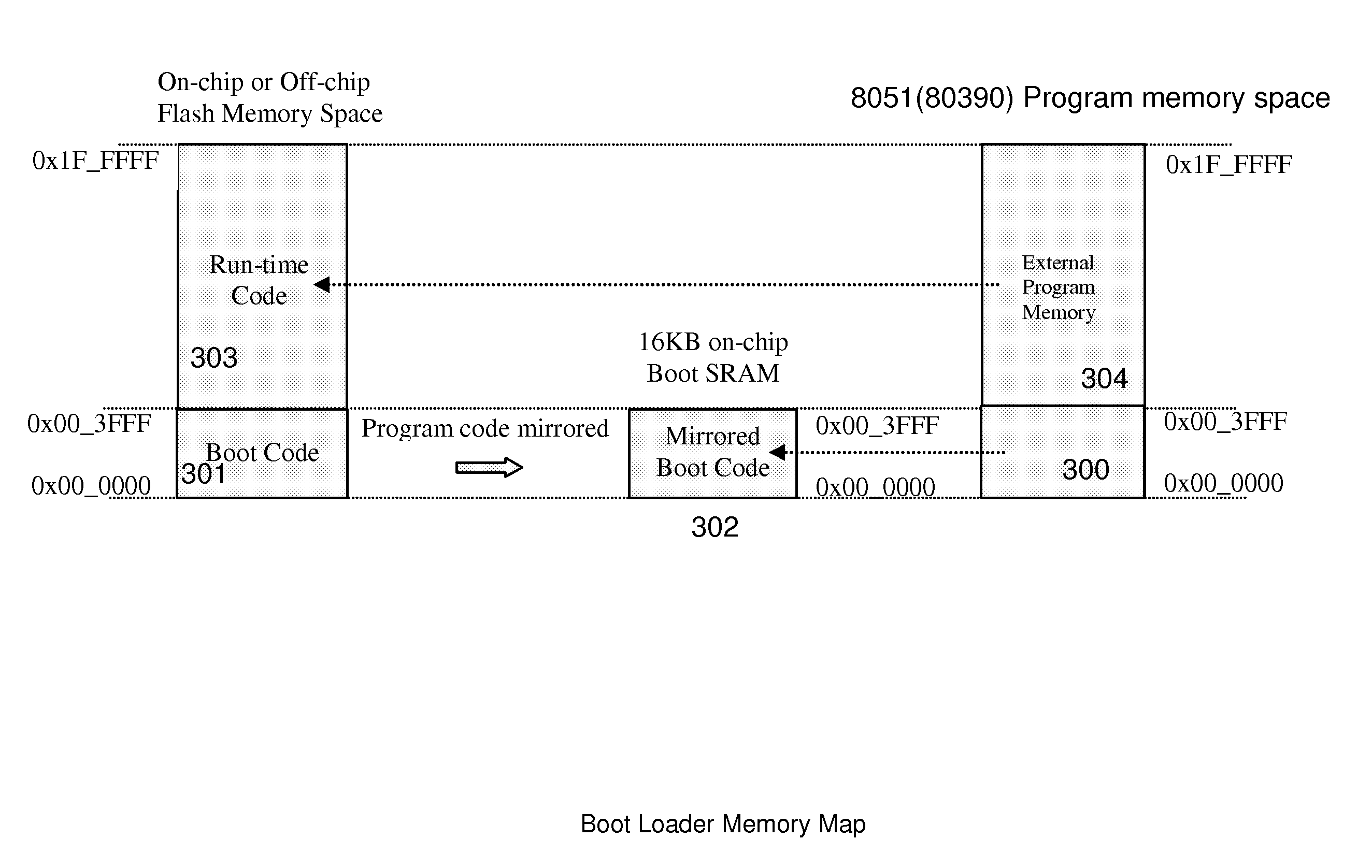
[0080]Step 2: Reading any program address space 16K˜32K (0x00—4000˜0x007FFF) will be remapped to the 0K˜16K (0x00—0000˜0x00—3FFF) address space of the Flash memory. Therefore, the memory content of lower 16 KB of the on-chip Flash memory can now be accessed. Note that the access of the 16 KB˜32 KB address space of Flash memory is temporarily disabled after step 1.
[0081]Step 3: After done with accessing the lower 16 KB of on-chip Flash memory, the software then writes FARM bit=0, to disable Flash memory address re-mapping mechanism. Now the access of program address space 16 KB˜32 KB would revert back to the same address space of the Flash memory as usual, and the access of 0K˜16K (0x00—0000˜0x00—3FFF) address space of the Flash memory is disabled again.
case 3
te the lower 16 KB (at 0x00—0000˜0x00—3FFF) of Flash memory 702:
[0082]Step 1: Software first writes PWE bit=1 in PCON SFR register, to enable program write in CPU.
[0083]Step 2: Software writes FARM bit=1 in CSREPR SFR register, to enable Flash memory address re-mapping mechanism. Now access of the 0K˜16K (0x00—0000˜0x00—3FFF) address space of the Flash memory would come from software accessing the program address space 16K˜32K (0x00—40000x007FFF).
[0084]Step 3: Programming sequence for performing Flash memory “Sector Erase” command:[0085]1. Write (0x4000+0x555)=0xAA[0086]2. Write (0x4000+0x2AA)=0x55[0087]3. Write (0x4000+0x555)=0x80[0088]4. Write (0x4000+0x555)=0xAA[0089]5. Write (0x4000+0x2AA)=0x55[0090]6. Write (0x4000+0x000)=0x30[0091]7. Repeatedly read (0x4000+0x3FFF). If equal to 0xFF, the Sector Erase command is completed.
[0092]Step 4: Programming sequence for performing Flash memory “Byte Program” command:[0093]1. Write (0x4000+0x555)=0xAA[0094]2. Write (0x4000+0x2AA)=0x55[009...
PUM
 Abstract
Description
Claims
Application Information
 - R&D
- Intellectual Property
- Life Sciences
- Materials
- Tech Scout
- Unparalleled Data Quality
- Higher Quality Content
- 60% Fewer Hallucinations
Browse by: Latest US Patents, China's latest patents, Technical Efficacy Thesaurus, Application Domain, Technology Topic, Popular Technical Reports.
© 2025 PatSnap. All rights reserved.Legal|Privacy policy|Modern Slavery Act Transparency Statement|Sitemap|About US| Contact US: help@patsnap.com


