Electron beam apparatus and image display apparatus using the same

a technology of image display and electron beam, which is applied in the manufacture of electrode systems, electric discharge tubes/lamps, and discharge tubes luminescnet screens, etc., can solve the problems of the amount of electrons to be emitted, and achieve the effects of high electron-emitting efficiency, simple structure and stable operation

Inactive Publication Date: 2011-02-08
CANON KK
View PDF79 Cites 4 Cited by
  • Summary
  • Abstract
  • Description
  • Claims
  • Application Information

AI Technical Summary

Benefits of technology

[0008]The present invention has been designed at solving the above described problems of a conventional technology, and is directed at providing an electron beam apparatus having an electron-emitting device provided therein, which has a simple structure, shows high electron-emitting efficiency and stably works.
[0012]According to the present invention, it is possible to selectively form a portion (strong portion) which has an increased electric-field strength in an electron-emitting device, and as a result, it is possible to easily control the position of electron-emitting points in a preferred embodiment.
[0013]The electron beam apparatus also can prevent emitted electrons from forming a leak current after having collided against the surface of the gate by covering the surface of the gate to be exposed to a recess portion of an insulating member with an insulating layer, and further can enhance its electron-emitting efficiency.
[0014]Furthermore, when having a plurality of cathodes with respect to the gate, the electron beam apparatus according to the present invention can control a shape of an electron beam to be emitted toward an anode, and provides a further stable electron-emitting action.
[0015]Still furthermore, the electron beam apparatus can make an emitted electron selectively collide against the humped portion, by providing the humped portion shorter than a width of the protruding portion of the cathode on the gate, and simultaneously can make a colliding portion of the emitted electron centralized on a side face of the humped portion. As a result, the electron after having collided against the side face flies to the anode without further colliding against other parts, so that the electron-emitting efficiency is further enhanced.
[0016]Therefore, the present invention realizes an electron beam apparatus provided with an electron-emitting device which has high electron-emitting efficiency and has a stable emitting action.

Problems solved by technology

However, the above electron-emitting devices do not solve a problem sufficiently that an amount of electron to be emitted from each of points of the electron-emitting points increases and decreases along with a driving period of time of driving a device, even though the technologies could inhibit the electric discharge in the electron-emitting portion.

Method used


Image

  • Electron beam apparatus and image display apparatus using the same
  • Electron beam apparatus and image display apparatus using the same
  • Electron beam apparatus and image display apparatus using the same

Examples


exemplary embodiment 1

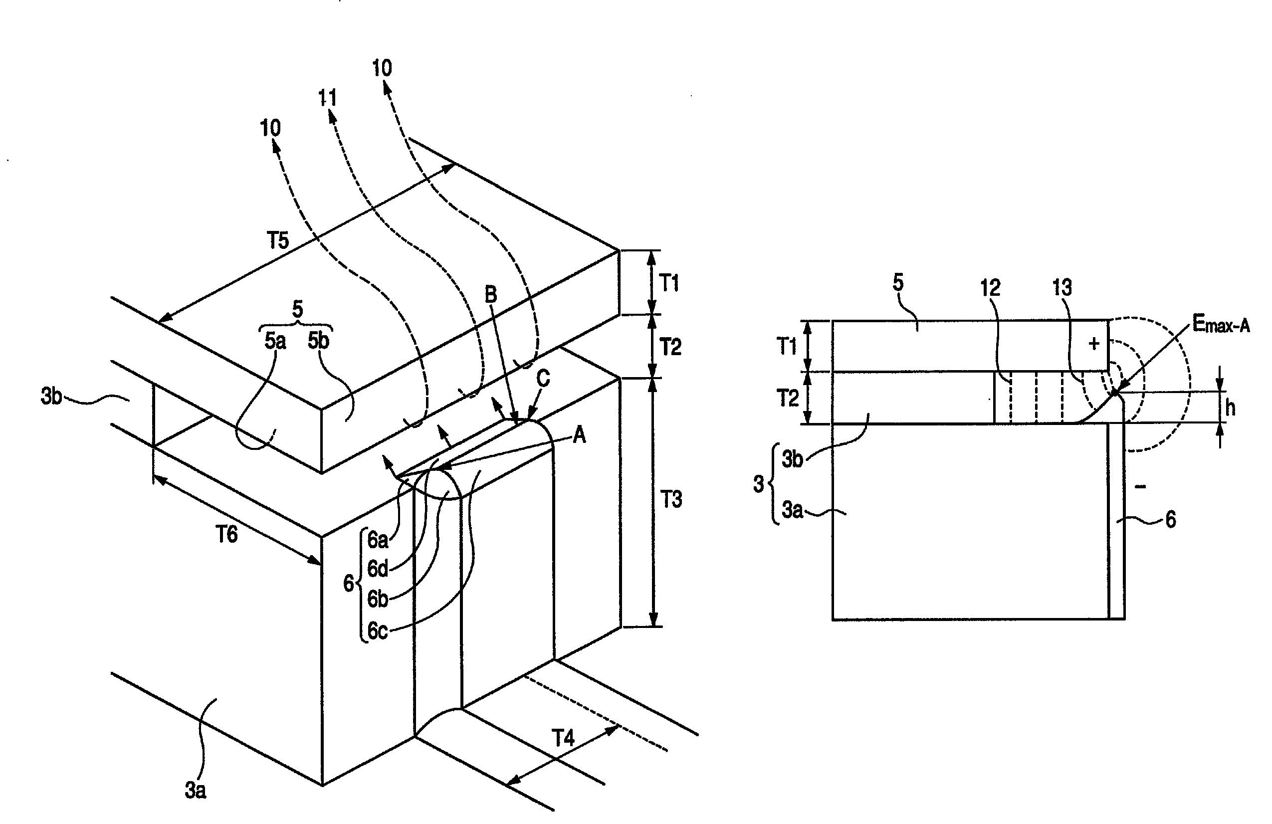
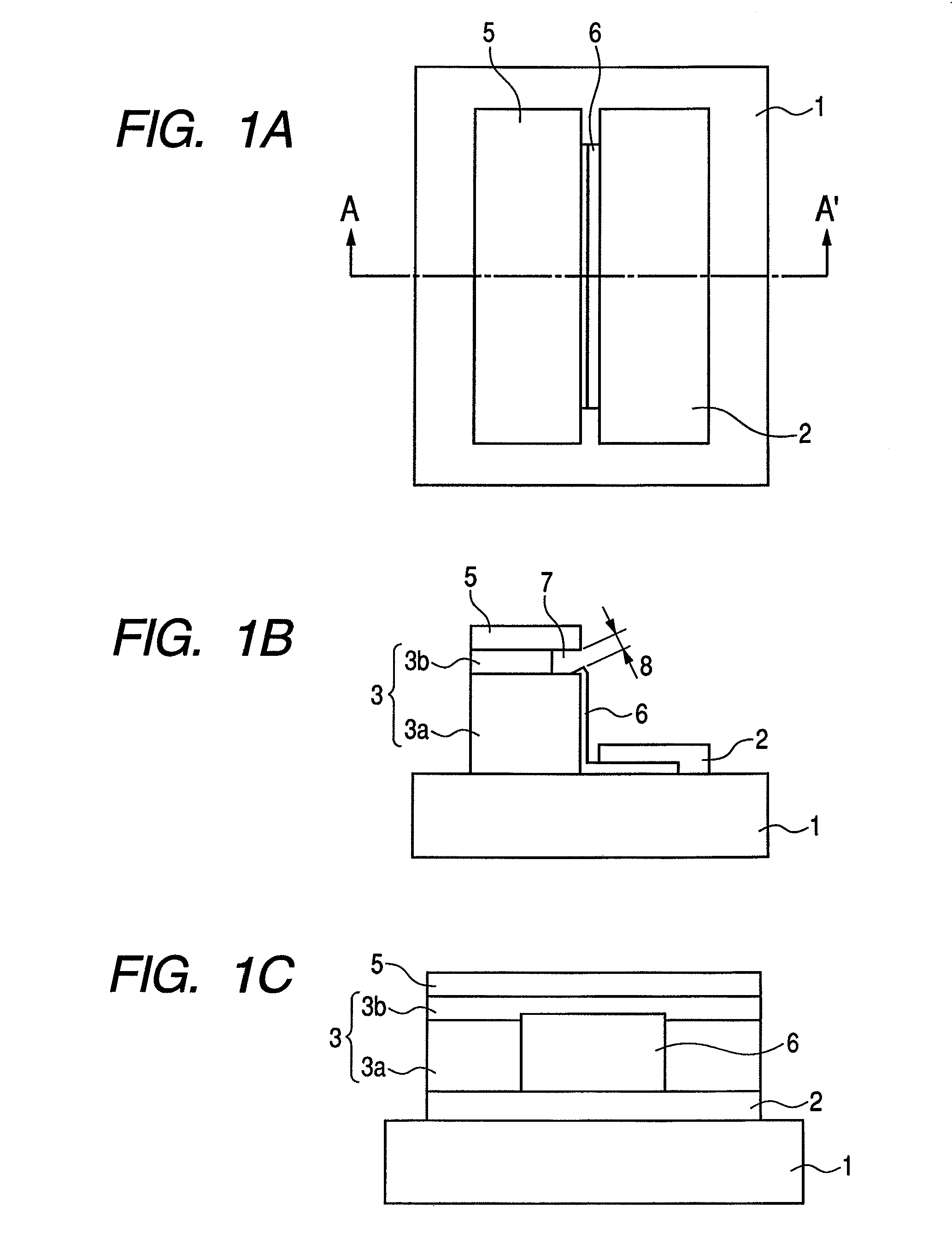
[0160]An electron-emitting device having a structure illustrated in FIGS. 1A to 1C was prepared according to the steps in FIGS. 14A-A to 14A-C and FIGS. 14B-D to 14B-F.

[0161]A PD200 was used for a substrate 1, which is low-sodium glass that has been developed for a plasma display, and SiN (SixNy) was formed thereon as an insulating layer 73 with a sputtering method so as to have a thickness of 500 nm. Subsequently, an SiO2 layer having a thickness of 30 nm was formed as an insulating layer 74 through a sputtering method. A TaN film having a thickness of 30 nm was stacked on the insulating layer 74 as an electroconductive layer 75 through a sputtering method (FIG. 14A-A).

[0162]Subsequently, a resist pattern was formed on the electroconductive layer 75 with a photolithographic technology, and the electroconductive layer 75, the insulating layer 74 and the insulating layer 73 were sequentially processed through a dry etching technique to form a gate 5 and an insulating member 3 which i...

exemplary embodiment 2

[0172]The electron-emitting device illustrated in FIGS. 15A to 15C was prepared. The basic preparing method is the same as in Exemplary embodiment 1, so that only the difference from that in Exemplary embodiment 1 will now be described below.

[0173]In the step of FIG. 14B-E, an EB vapor deposition method was employed as a method of forming a molybdenum film, and a substrate 1 was set at the angle of 80 degrees with respect to a horizontal plane. Thereby, Mo was incident on the upper part of a gate 5 at 80 degrees, and was incident on a slope face of the insulating member 3 which had been subjected to an RIE processing, at 20 degrees. Mo was formed so as to have the thickness of 20 nm on the slope face, by fixing the vapor deposition speed at approximately 10 nm / min during vapor deposition, and precisely controlling the vapor deposition period of time to 2 minutes.

[0174]After the Mo film was formed, the Mo film on the gate 5 was peeled by removing an Ni release layer 81 which had been...

exemplary embodiment 3

[0180]The electron-emitting device illustrated in FIGS. 16A to 16C was prepared. The basic preparing method is the same as in Exemplary embodiment 1, so that only the difference from the method in Exemplary embodiment 1 will now be described below.

[0181]SiO2 was deposited so as to have the thickness of 40 nm as an insulating layer 74 with a sputtering method, and TaN was deposited so as to have the thickness of 40 nm as an electroconductive layer 75 with a sputtering method.

[0182]An insulating layer 73, the insulating layer 74 and the electroconductive layer 75 were dry-etched by an RIE process in a similar way to that in Exemplary embodiment 1. The side face of an insulating member 3 and a gate 5 after having been etched was formed so as to have the angle of 80 degrees with respect to a substrate 1. Subsequently, a recess portion 7 was formed in the insulating member 3, by etching only the side face of an insulating layer 3b so as to form the recess portion with a depth of approxim...


PUM


Abstract

The present invention provides an electron beam apparatus provided with an electron-emitting device which has a simple structure, shows high electron-emitting efficiency and stably works. This electron beam apparatus has an insulating member and a gate formed on a substrate, a recess portion formed in the insulating member, a protruding portion that protrudes from an edge of the recess portion toward the gate and is provided on an end part of a cathode opposing to the gate, which is arranged on the side face of the insulating member; and makes an electric field converge on an end part in the width direction of the protruding portion to make an electron emitted therefrom.

Description

BACKGROUND OF THE INVENTION[0001]1. Field of the Invention[0002]The present invention relates to an electron beam apparatus which is used for a flat panel display and has an electron-emitting device that emits an electron provided therein.[0003]2. Description of the Related Art[0004]Conventionally, there is an electron-emitting device which makes a large number of electrons to be emitted from a cathode, collide against a facing gate and be scattered therein, and then takes out the electron. A surface conduction type electron-emitting device and a stacked type electron-emitting device are known as a device which emits an electron in such a form, and Japanese Patent Application Laid-Open No. 2000-251643 discloses a high-efficiency electron-emitting device in which a gap of an electron-emitting portion is 5 nm or less. In addition, Japanese Patent Application Laid-Open No. 2001-229809 discloses a stacked type electron-emitting device, in which conditions of enabling electron emission w...

Claims


Application Information

Patent Timeline
Patent Type & Authority Patents(United States)
IPC IPC(8): H01J1/304H01J1/30H01J19/34H01J19/38H01J19/02
CPCH01J9/025H01J29/467H01J31/127
Inventor TSUKAMOTO, TAKEOMORIGUCHI, TAKUTOTAKEUCHI, EIJI
Owner CANON KK
Why Eureka
Try Eureka