
Memory access system

a memory access and memory technology, applied in the field of memory access systems, can solve the problems of unintended rewriting of programs, inapplicability, and inability to recover the function of unselected cells, so as to avoid or reduce the phenomenon of read disturb, prevent frequent error detection, and reduce burden

Active Publication Date: 2011-01-25
MEGACHIPS
View PDF9 Cites 13 Cited by
  • Summary
  • Abstract
  • Description
  • Claims
  • Application Information

AI Technical Summary

Benefits of technology

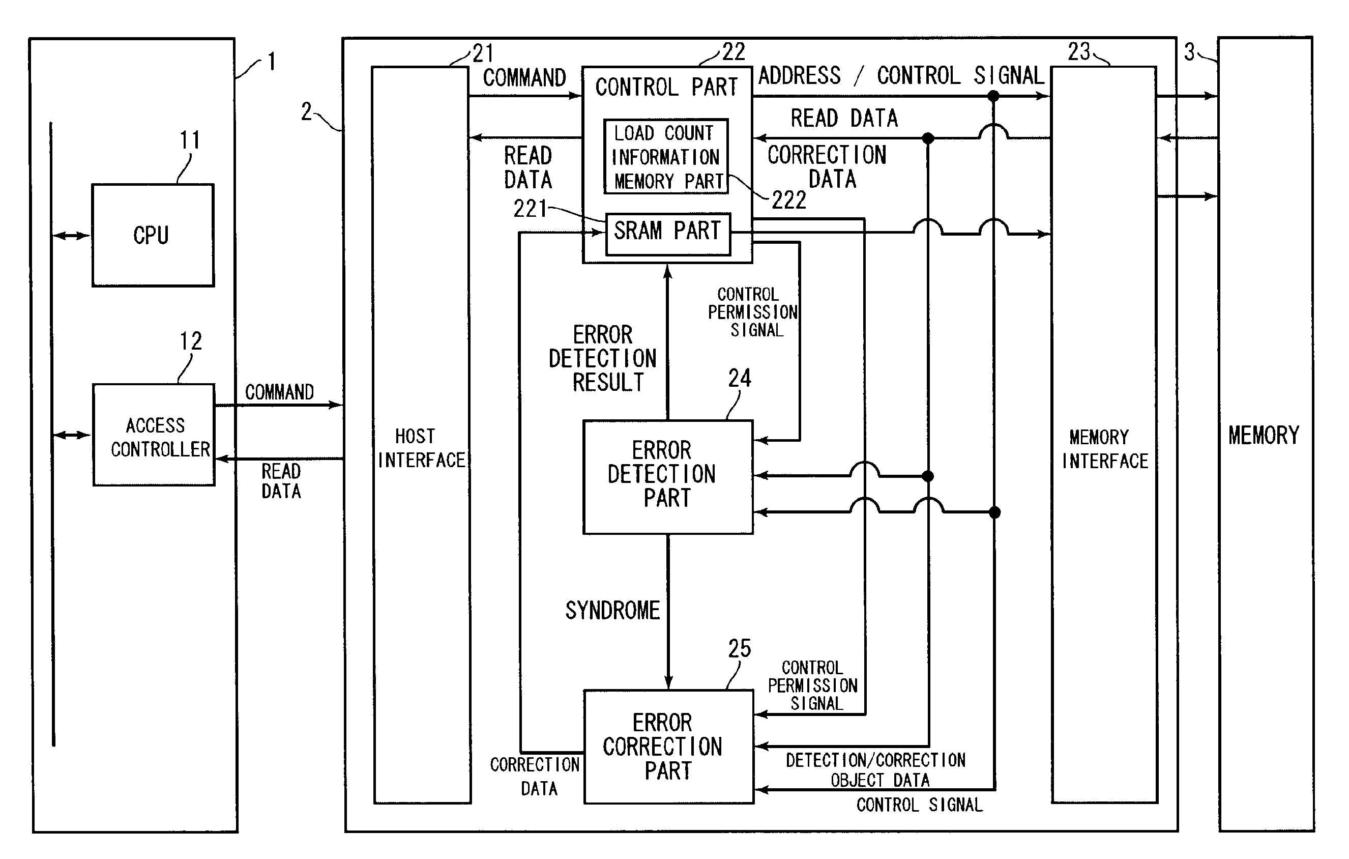
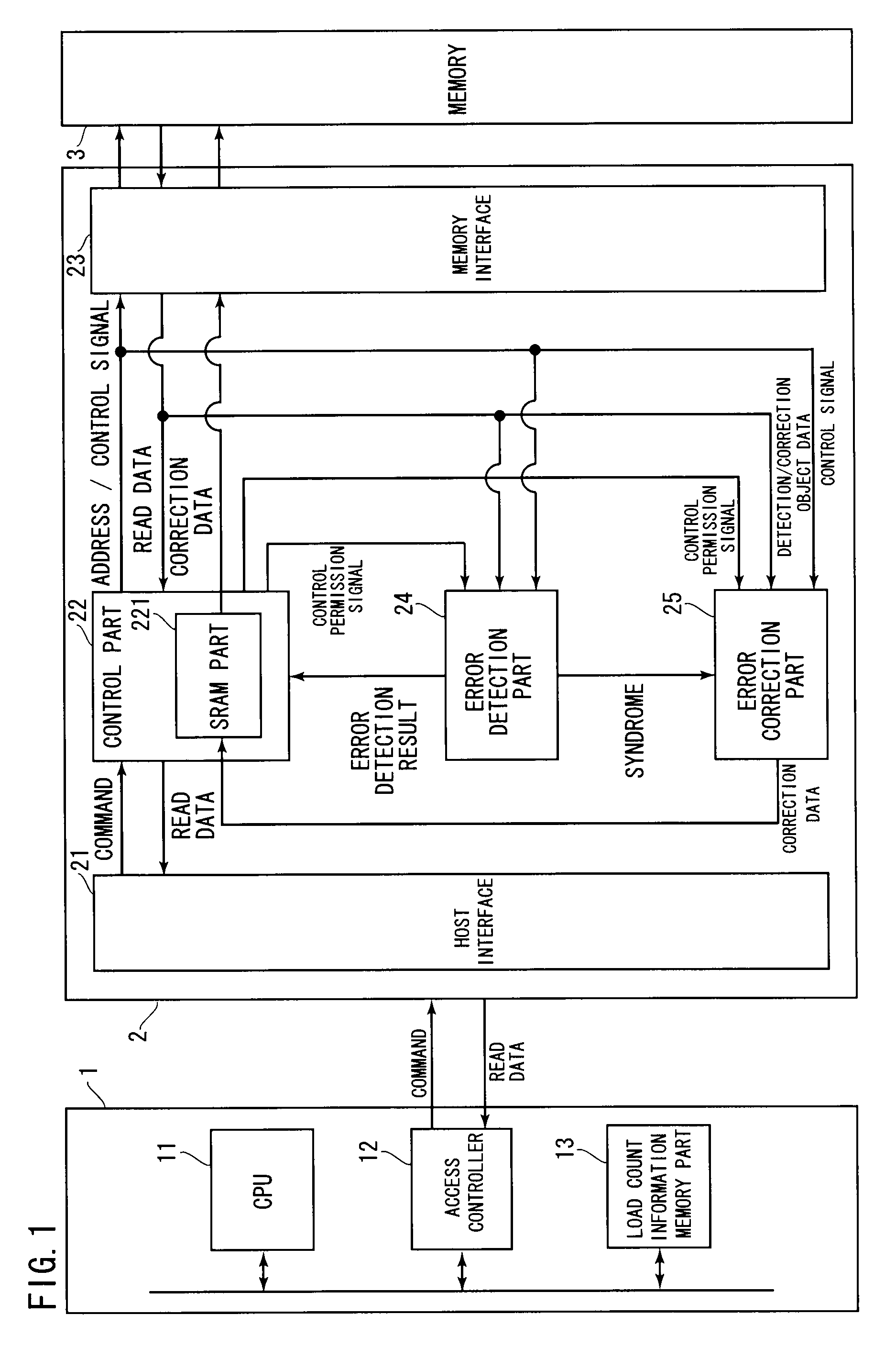
[0013]In this aspect of the present invention, the error detection and the error correction are performed not only on a selected cell associated with a read address but also on an unselected cell other than the selected cell associated with the read address. This avoids or reduces the read disturb phenomenon.
[0015]By this aspect of the present invention, it is possible to prevent the error detection from being performed on an error detection area immediately after the error correction is performed on the error detection area. This avoids or reduces the read disturb phenomenon with no burden imposed on the memory access system.
[0017]By this aspect of the present invention, it is possible to prevent frequent error detections. This avoids or reduces the read disturb phenomenon with no burden imposed on the memory access system.
[0018]Therefore, it is an object of the present invention to provide means for avoiding or reducing the read disturb phenomenon even in various types of nonvolatile memories without any restriction depending on cell configurations of memories.

Problems solved by technology

Since specific programs are repeatedly read out in the game machines or the like in most cases, however, it begins to be noticed that the programs could be unintendedly rewritten.
But, if there occurs no write operation and only consecutive read operations, it is impossible to recover the function of the unselected cell 53.
This disclosed method, however, can be applied to a memory having a specific cell configuration but can not be applied to any other cell configuration.
In other words, by this method, it is impossible to avoid the read disturb phenomenon without depending on cell configurations of memories.

Method used


Image

  • Memory access system
  • Memory access system
  • Memory access system

Examples


Embodiment Construction

4 is a flowchart showing an operation flow for error correction;

[0024]FIG. 5 is a flowchart showing an operation flow for writing of error correction data;

[0025]FIGS. 6A and 6B are views showing a manner of counting a load count in a NAND flash memory of the SLC system;

[0026]FIGS. 7A to 7C are views showing a manner of counting a load count in a NAND flash memory of the MLC system;

[0027]FIG. 8 is a schematic view of a NAND flash memory; and

[0028]FIG. 9 is a block diagram showing a memory system in accordance with an embodiment of the present invention.

DESCRIPTION OF THE PREFERRED EMBODIMENTS

Constituent Elements of Memory System Of This Preferred Embodiment

[0029]Hereinafter, the preferred embodiment of the present invention will be discussed with reference to figures. In the read disturb phenomenon, when data stored in a reading area is repeatedly read out, there is a possibility that data stored in a non-reading area might be unintendedly rewritten. Then, a memory system of this pre...


PUM


Abstract

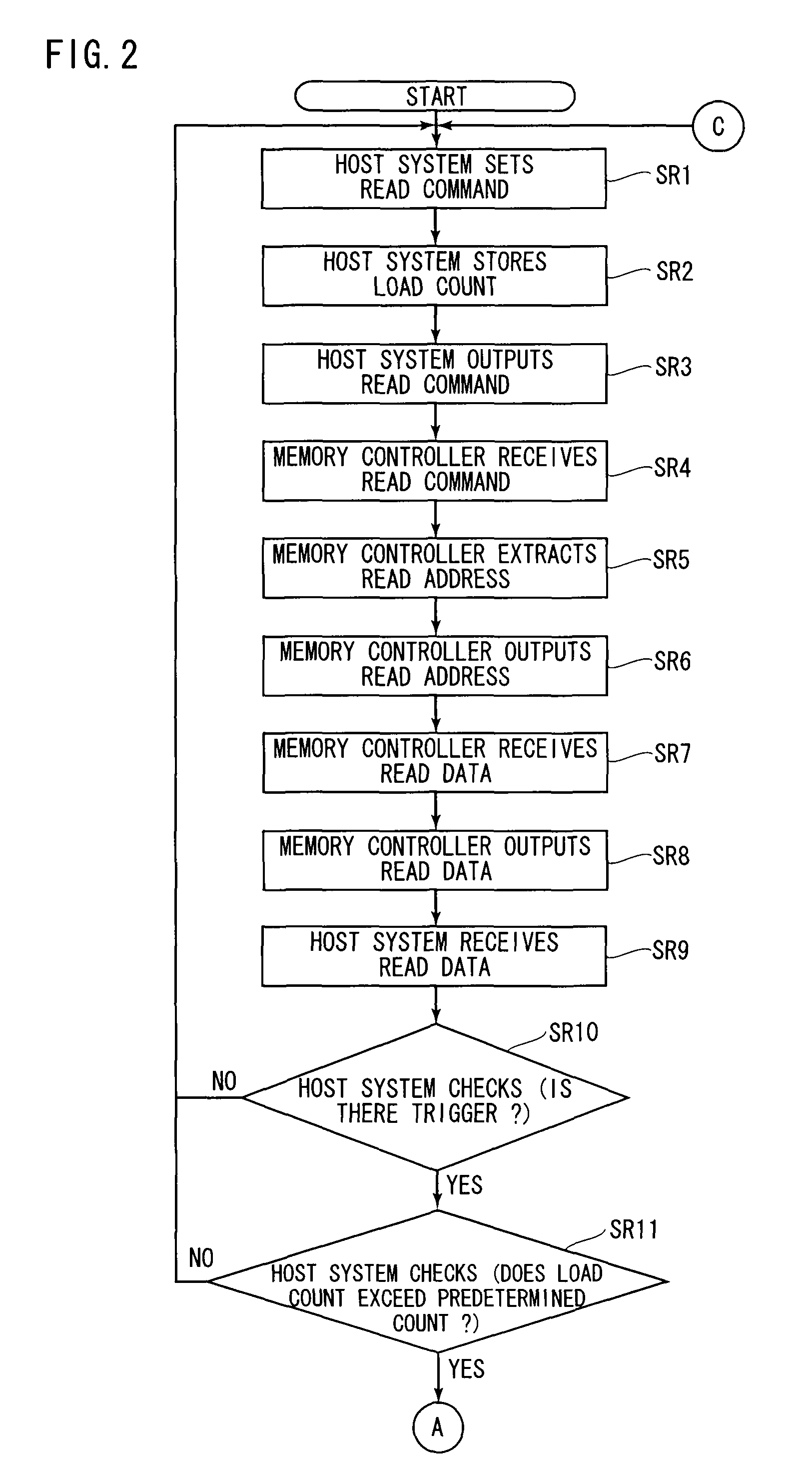
When a host system outputs a read command to a memory controller, it measures a load count of a memory area on which a read access load is imposed. Then, when the host system judges that the load count of a memory area reaches a predetermined count, it causes the memory controller to perform an error detection on the memory area. Further, when the host system finds that an error occurs in the memory area, it causes the memory controller to perform an error correction on the memory area. This can avoid or reduce unintended rewriting due to repeated readouts.

Description

BACKGROUND OF THE INVENTION[0001]1Field of the Invention[0002]The present invention relates to a technique to avoid unintended rewriting of data or reduce the possibility thereof, due to repeated readouts of data from a nonvolatile memory.[0003]2. Description of the Background Art[0004]NAND flash memories, among nonvolatile memories, are heavily used for SD memory cards or the like for the purpose of achieving high integration, reduction in manufacturing cost and easy writing for users by simplifying circuit configurations.[0005]In recent, NAND flash memories are adopted for game machines or the like. When the NAND flash memories are used for game machines, there occurs no write operation but only consecutive read operations. In other words, NAND flash memories have been increasingly adopted as ROMs.[0006]Since specific programs are repeatedly read out in the game machines or the like in most cases, however, it begins to be noticed that the programs could be unintendedly rewritten. ...

Claims


Application Information

Patent Timeline
Patent Type & Authority Patents(United States)
IPC IPC(8): G11C29/00
CPCG06F11/1068G11C16/0483G11C2029/0411
Inventor SUGAHARA, TAKAHIKO
Owner MEGACHIPS
Learn More