Shift register and liquid crystal display device using the same
a technology of shift register and liquid crystal display, which is applied in the direction of digital storage, instruments, computing, etc., can solve the problems of crt having limitations in both size and weigh
- Summary
- Abstract
- Description
- Claims
- Application Information
AI Technical Summary
Benefits of technology
Problems solved by technology
Method used
Image
Examples
first embodiment
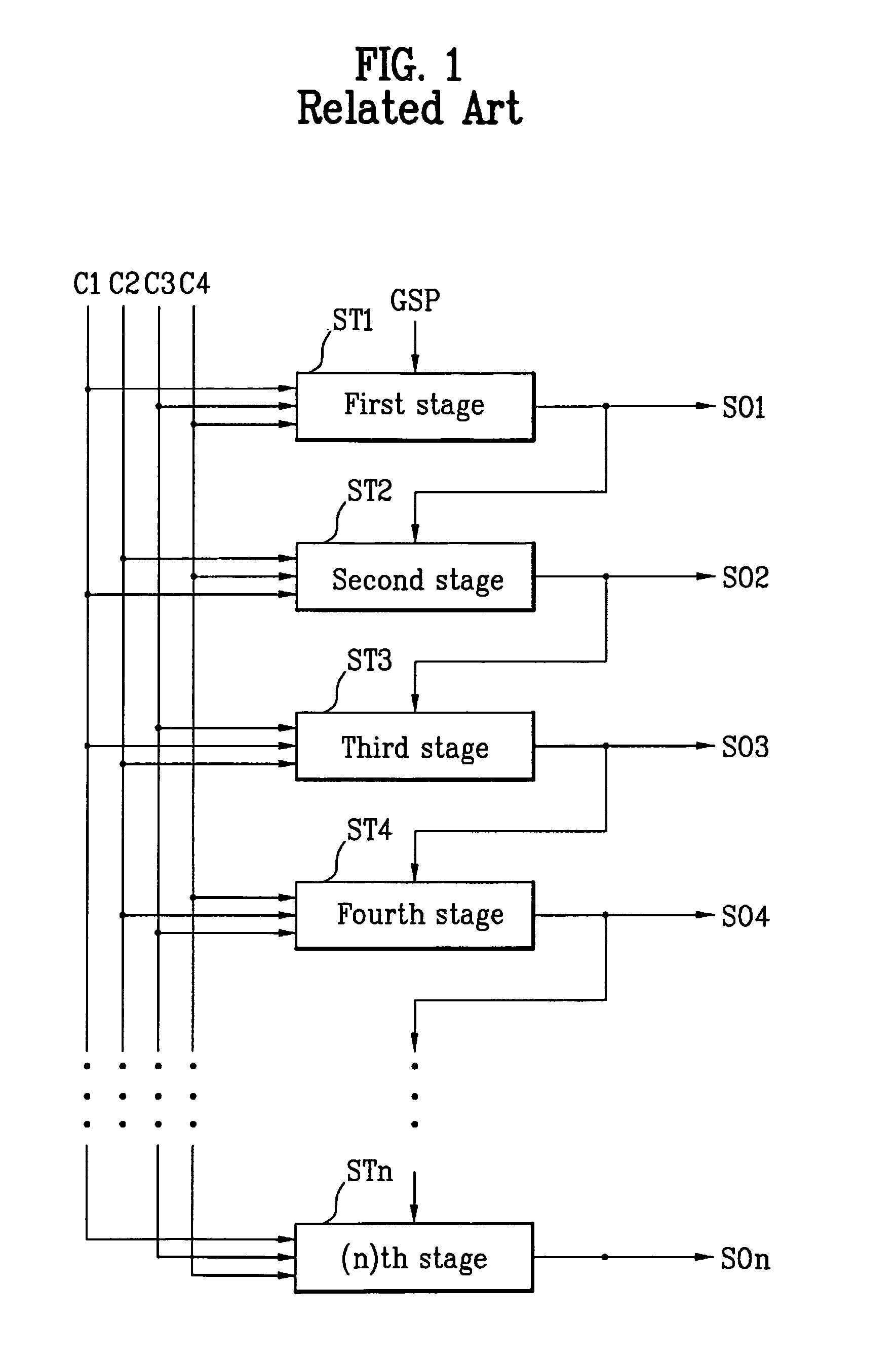
[0057]FIG. 7 is the schematic view showing the shift register 120 of the gate driver 114 shown in FIG. 5. Referring to FIG. 7, the shift register 120 according to the present invention is comprised of ‘n’ stages ST1 to STn which are connected with gate start pulse input lines, for receiving three clock signals among four clock signals C1 to C4 and the first to third supplying voltages VDD1, VDD2, and VSS outputted from the voltage generator 118.
[0058]The first stage ST1 outputs a first output signal S01 using the gate start pulse GSP and three clock signals among the four clock signals C1 to C4, such as C1, C3, and C4. Then, the second to n-th stages ST2 to STn respectively output second to n-th output signals S02 to S0n using the output signal S01 to S0n−1) outputted from each prior stage ST1 to ST(n−1) and three clock signals among the four clock signals C1 to C4. That is, the first to n-th stages ST1 to STn sequentially output the first to n-th output signals S01 to S0n of which ...
second embodiment
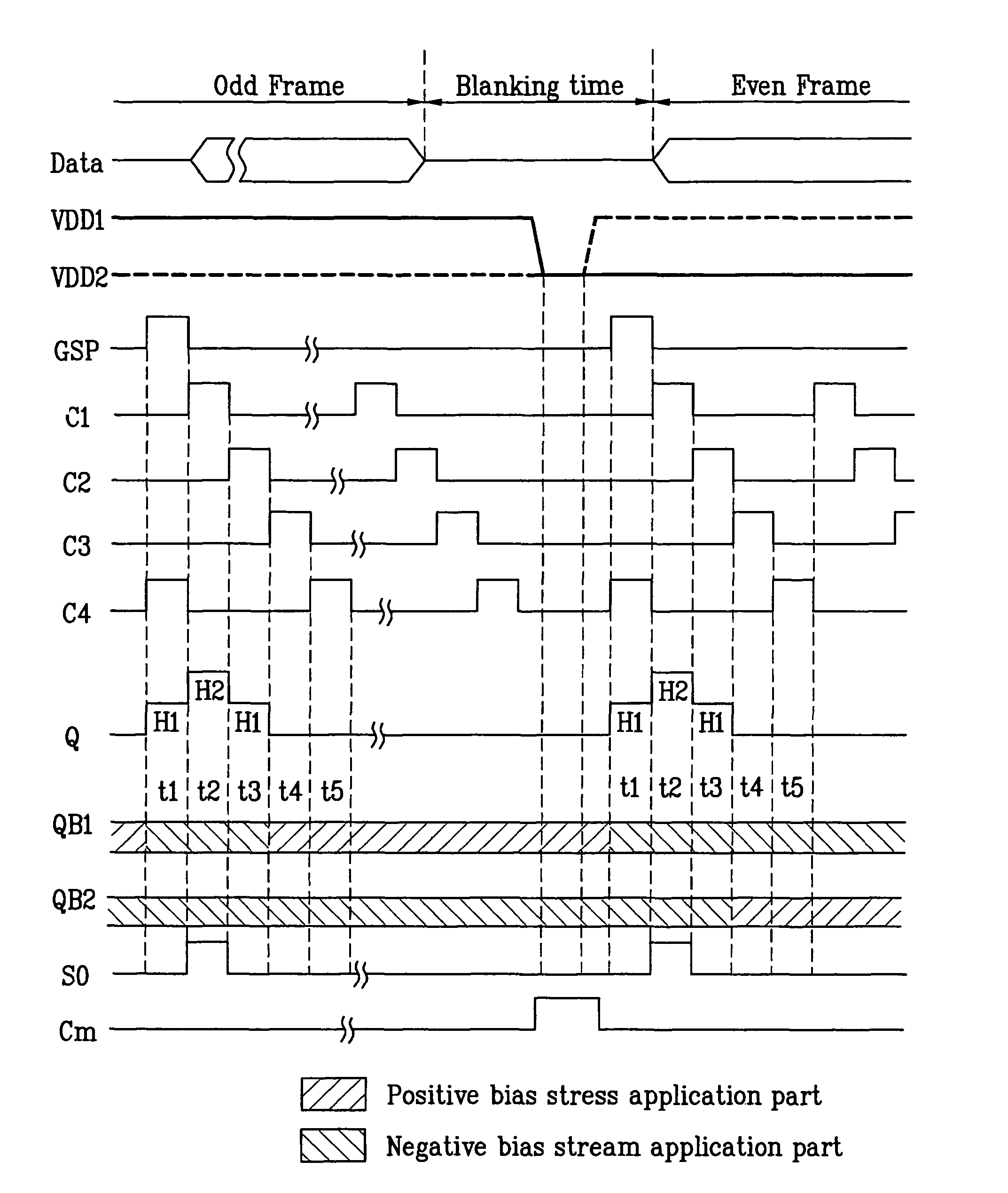
[0102]After outputting the signal from each of ‘n’ stages ST1 to STn, the first to fourth clock signals C1 to C4 are in the low state by the clock mask signal Cm in some period of the blanking time which corresponds to the interval between the frames, whereby it is possible to prevent the bias stress from being applied to the respective transistors T. In the shift register and the LCD device according to the present invention, it is possible to prevent the bias stress from being applied to the transistor by the continuous logic change of the clock signals C1 to C4, and to prevent the transistor from being deteriorated.
[0103]During some sections of the blanking time, the first supplying voltage VDD1 of the high state, supplied to the shift register 220, is inversed to the low state, and the second supplying voltage VDD2 of the low state is inversed to the high state.
[0104]In the even-numbered frame, the fifth and eighth transistors T15 and T18 are maintained in the turn-on state by t...
PUM
 Abstract
Description
Claims
Application Information
 - R&D
- Intellectual Property
- Life Sciences
- Materials
- Tech Scout
- Unparalleled Data Quality
- Higher Quality Content
- 60% Fewer Hallucinations
Browse by: Latest US Patents, China's latest patents, Technical Efficacy Thesaurus, Application Domain, Technology Topic, Popular Technical Reports.
© 2025 PatSnap. All rights reserved.Legal|Privacy policy|Modern Slavery Act Transparency Statement|Sitemap|About US| Contact US: help@patsnap.com


