
Gate electrode with depletion suppression and tunable workfunction

a technology of depletion suppression and workfunction, applied in the field of semiconductor devices, can solve the problems of increasing complexity, increasing circuit density and complexity, and reducing power consumption and package sizes of integrated circuit devices, so as to reduce the effect of gate depletion effect, low gate resistivity, and high performance mosfets

Inactive Publication Date: 2011-01-11
THE BOARD OF TRUSTEES OF THE LELAND STANFORD JUNIOR UNIV
View PDF11 Cites 2 Cited by
  • Summary
  • Abstract
  • Description
  • Claims
  • Application Information

AI Technical Summary

Benefits of technology

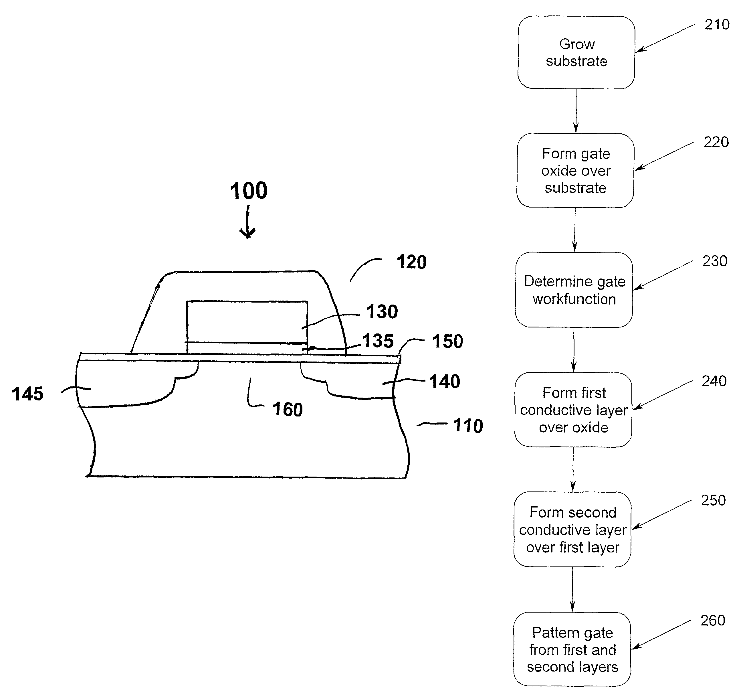
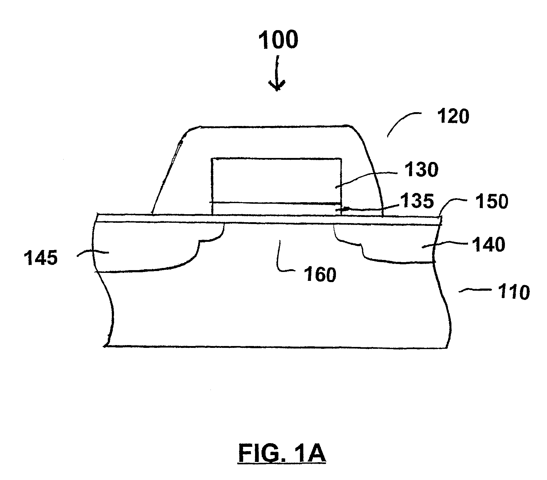
[0011]In one example embodiment of the present invention, a structure is adapted to enable tuning of the effective workfunction of a gate electrode by adjusting the thickness (an independent property) of a lower layer of the gate electrode, when two selected materials are used to faun upper and lower layers in the gate electrode. Thus, desired device properties including low gate carrier depletion, low gate resistivity, proper effective gate workfunction, and appropriate channel region doping and composition can be optimized simultaneously, thereby enabling higher performance MOSFETs.
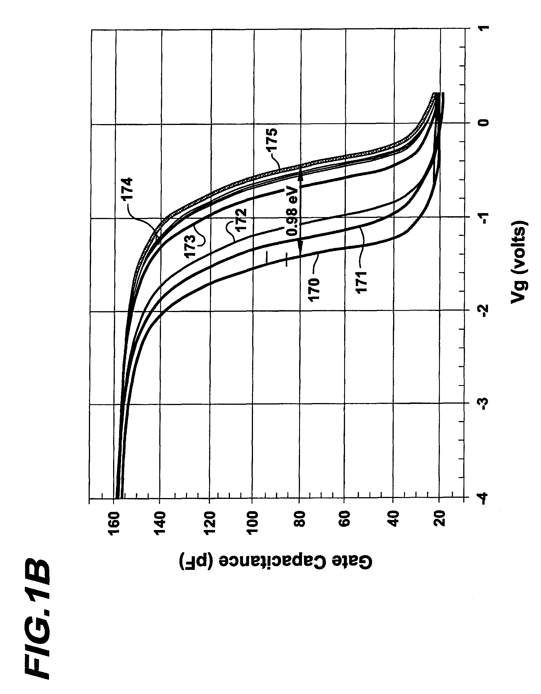
[0012]According to a more particular example embodiment of the present invention, a semiconductor device structure is manufactured with a gate electrode that consists of a thin lower layer and a thicker upper layer. The respective workfunctions of the two layers are chosen to be sufficiently different and the order of layers is arranged such that the carriers, either electrons or holes, will be injected toward the lower layer by the difference between the workfunctions of the two materials. The redistribution of carriers (e.g., electrons or holes) toward the lower layer will shift the effective workfunction of the composite gate electrode to a value that is between that of the bulk workfunctions of the lower and upper layer materials. In the case where the lower layer has a thickness of only a few atomic spacings, the resulting effective workfunction of the composite gate electrode will be closer to the value of the upper layer material. When the thickness of lower layer is increased, the effective workfunction of the composite gate electrode will shift toward to that of the lower layer material. By choosing the thickness of the lower layer, the effective workfunction of the composite gate electrode can be tuned to a value between the bulk workfunctions of the upper and lower layer materials. Specifically, the two materials are selected such that a sufficient workfunction difference exists between them, and two layers of the materials are ordered to achieve the workfunction. The action of carrier redistribution (either electrons or holes) toward the lower layer will also reduce gate depletion effects, thereby improving the device current drive.

Problems solved by technology

Recent technological advances in the semiconductor industry have permitted dramatic increases in circuit density and complexity, and commensurate decreases in power consumption and package sizes for integrated circuit devices.
These and other demands have led to increased pressure to manufacture a large number of semiconductor devices at an efficient pace while increasing the complexity and improving the reliability of the devices.
The superposition of both doping profiles causes excess dopant to be situated within the channel region, and so degrades the mobility of carriers and reduces transistor speed.
In addition, for MOSFET applications where the channel length would be scaled down to sub-70 nanometers (nm), it becomes very difficult to simultaneously optimize both the punch-through-suppression doping and the threshold-adjustment doping profiles.
In addition, the discrete distribution of implanted dopants can cause large deviations in threshold voltage from device to device, for sub-70 nm channel lengths, which represents a fundamental limitation to the scaling of MOSFETs.
For such applications, however, the adjustment is possible only within a limited range, and is only applicable to p-MOSFETs.
Furthermore, these alloys suffer from a drawback of manufacturing a gate electrode from a semiconductor (either polysilicon or poly-silicon-germanium); namely these gate electrodes have an electrical carrier concentration that is usually limited to the order of about 1020 cm−3.
Consequently, gate capacitance is reduced, which in turn reduces the transistor's current drive and speed.
Implementations of such metal gate electrodes have been difficult due to the lack of availability of appropriate workfunction values and / or due to chemical instability.
Thus, the use of metallic gate electrodes has been hindered.
This limitation and others discussed herein have been a challenge in the semiconductor industry.

Method used


Image

  • Gate electrode with depletion suppression and tunable workfunction
  • Gate electrode with depletion suppression and tunable workfunction
  • Gate electrode with depletion suppression and tunable workfunction

Examples


Embodiment Construction

[0023]The present invention is believed to be applicable to a variety of different types of semiconductor devices, and the invention has been found to be particularly suited for devices in the deep-sub-micron regime, such as MOS devices, thyristors and other structures including a gate electrode over an underlying substrate. While the present invention is not necessarily limited to such applications, various aspects of the invention may be appreciated through a discussion of various examples using this context.

[0024]According to an example embodiment of the present invention, a gate electrode having a tunable effective workfunction is formed in a semiconductor device. At least two conductive materials are used in a selected arrangement to form the gate electrode, and the arrangements are selected to achieve an effective gate workfunction that provides a selected threshold voltage for the device. The gate is adapted to be formed in one of a plurality of configurations, each configura...


PUM


Abstract

Semiconductor device performance is improved via a gate structure having a tunable effective workfunction and reduced gate depletion effects. According to an example embodiment, the design threshold voltage of a semiconductor device is adjusted in a manner that includes providing a gate having a workfunction that enables operation of the semiconductor device at a selected voltage. The gate is formed having two different conductive materials with different electric workfunctions that both significantly contribute to the overall workfunction of the gate. The relative composition, thickness, and arrangement of each of the two conductive materials is selected to attain a gate electrode workfunction that is different than the workfunctions of each of the two layers and that sets the threshold voltage of the semiconductor device. The adjustability of the effective workfunction of the gate electrode can be applied to a variety of semiconductor devices. The ability to reduce gate depletion effects also provides enhanced device current drive.

Description

RELATED PATENT DOCUMENTS[0001]This is a divisional (or alternatively, a continuation) under 35 U.S.C. §120 of U.S. patent application Ser. No. 11 / 605,714 filed on Nov. 29, 2006, which is a divisional of U.S. patent application Ser. No. 10 / 450,476 filed on Jan. 16, 2004 now abandoned, which is the national stage entry under 35 U.S.C. 371 of International Application No. PCT / US2001 / 030926 filed on Oct. 2, 2001, which claims benefit under 35 U.S.C. §119(e) of U.S. Provisional Application Ser. No. 60 / 256,708 filed on Dec. 18, 2000; each of these patent documents is fully incorporated herein by reference.FIELD OF THE INVENTION[0002]The present invention relates generally to semiconductor devices having a gate structure whereby the thickness and structure of the gate electrode material are used to minimize gate depletion effects and to tune the gate workfunction, e.g., thereby setting a threshold voltage of a transistor.BACKGROUND OF THE INVENTION[0003]Recent technological advances in the...

Claims


Application Information

Patent Timeline
Patent Type & Authority Patents(United States)
IPC IPC(8): H01L21/336H01L21/20H01L21/4763H01L21/3205H01L21/28H01L29/10H01L29/49
CPCH01L21/28079H01L29/1054H01L29/4958
Inventor HUNG, STEVENHOYT, JUDY L.GIBBONS, JAMES F.
Owner THE BOARD OF TRUSTEES OF THE LELAND STANFORD JUNIOR UNIV
Learn More