Method and apparatus for producing biaxially oriented thin films

a thin film, biaxial crystal technology, applied in the direction of instruments, heat measurement, therapy, etc., can solve the problems of not much room in the known apparatus, weak efficiency of the known ibad method of producing thin films with the desired biaxial crystal orientation, and limited range of argon ions within the thin film. only a few nanometers

Inactive Publication Date: 2010-11-09
BRUKER HTS
View PDF4 Cites 2 Cited by
  • Summary
  • Abstract
  • Description
  • Claims
  • Application Information

AI Technical Summary

Benefits of technology

[0010]With the novel method and apparatus, it is possible to produce thin films having an improved biaxial crystal orientation compared to thin films of the same thickness being produced by the IBAD method. Furthermore, the spatial limitations known from the IBAD method due to the overlapping working regions of the source for atoms and the source for an energized laser beam are overcome.
[0017]In the novel method, it is furthermore preferred if non-continuous clusters of atoms are deposited on the substrate and on the previously deposited atoms, respectively, during each step of depositing atoms. Thus, in each step of depositing, it is desired not to deposit continuous regions of atoms, but instead separate single groups. When these non-continuous clusters of atoms are then bombarded by an energized beam, they are completely removed with an especially high probability. In this way, a high concentration of the texture having the desired biaxial crystal orientation is realized in the thin film very quickly.
[0020]When the substrate is guided to move along a circular path or a spiral path, it is especially preferred if the substrate is located in a plane in each portion in which a step of bombarding the deposited atoms with an energized beam is realized. In this way, especially favorable conditions for attaining the desired biaxial crystal orientation by the energized beam are realized. In case the substrate is oriented in a sloped way in this portion, there are substantially less constant and thus less advantageous angle conditions. For each region in which a step of depositing atoms on the substrate is realized, it is also advantageous if the substrate is oriented in a plane.
[0022]Furthermore, the energized beam does not have to have an identical design and orientation during each step of bombarding the deposited atoms. Instead, it is possible to vary the beam with respect to its kind, its composition, its energy, its power and / or its angle of orientation with respect to the substrate in between the steps. However, usually, the beam is not varied in between the consecutive steps of bombarding the deposited atoms.
[0028]To increase the total volume of the biaxially oriented thin film which can be produced by the novel apparatus during a certain period of time, it is possible to arrange a plurality of sources for atoms and a plurality of sources for energized beams as pairs one after the other in the direction of the path on which the substrate is moved by the drive. The plurality of sources for atoms may be identical, or sources may be different. However, usually they are identical. Certain cases are imaginable in which different sources produce thin films of special quality. The same applies to the plurality of sources for an energized beam.

Problems solved by technology

Thus, there is not much room in the known apparatus, especially when the sources are located comparatively close to the substrate.
Due to the fact that the increase of thickness of a thin film being produced by the IBAD method is small, the efficiency of the known IBAD method of producing thin films with the desired biaxial crystal orientation is strongly limited.
However, the range of the argon ions within the thin film only is a few nanometers.
Even then, the known method only realizes a biaxial texture to a small extent.
This comparatively bad result of the desired biaxial crystal orientation is not compensated by the fact that—due to conducting the steps of depositing and of bombarding the deposited atoms with an energized beam at different points in time—these steps may also be conducted at different locations such that the source for atoms and the source for an energized beam do not interfere although their working ranges overlap in the desired way.

Method used


Image

  • Method and apparatus for producing biaxially oriented thin films
  • Method and apparatus for producing biaxially oriented thin films
  • Method and apparatus for producing biaxially oriented thin films

Examples


example 1

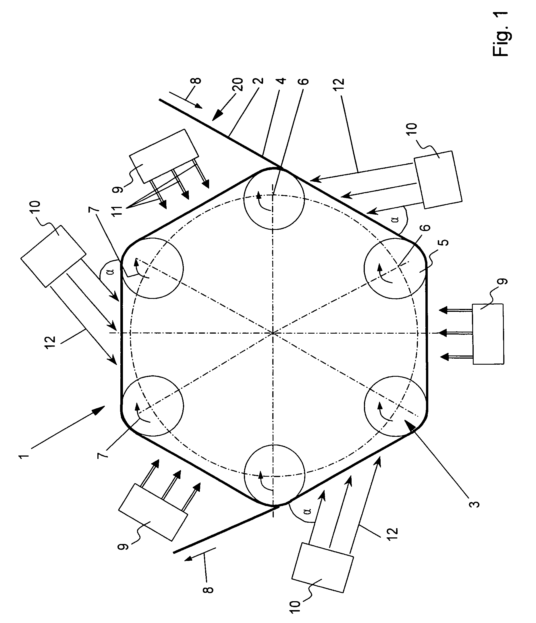
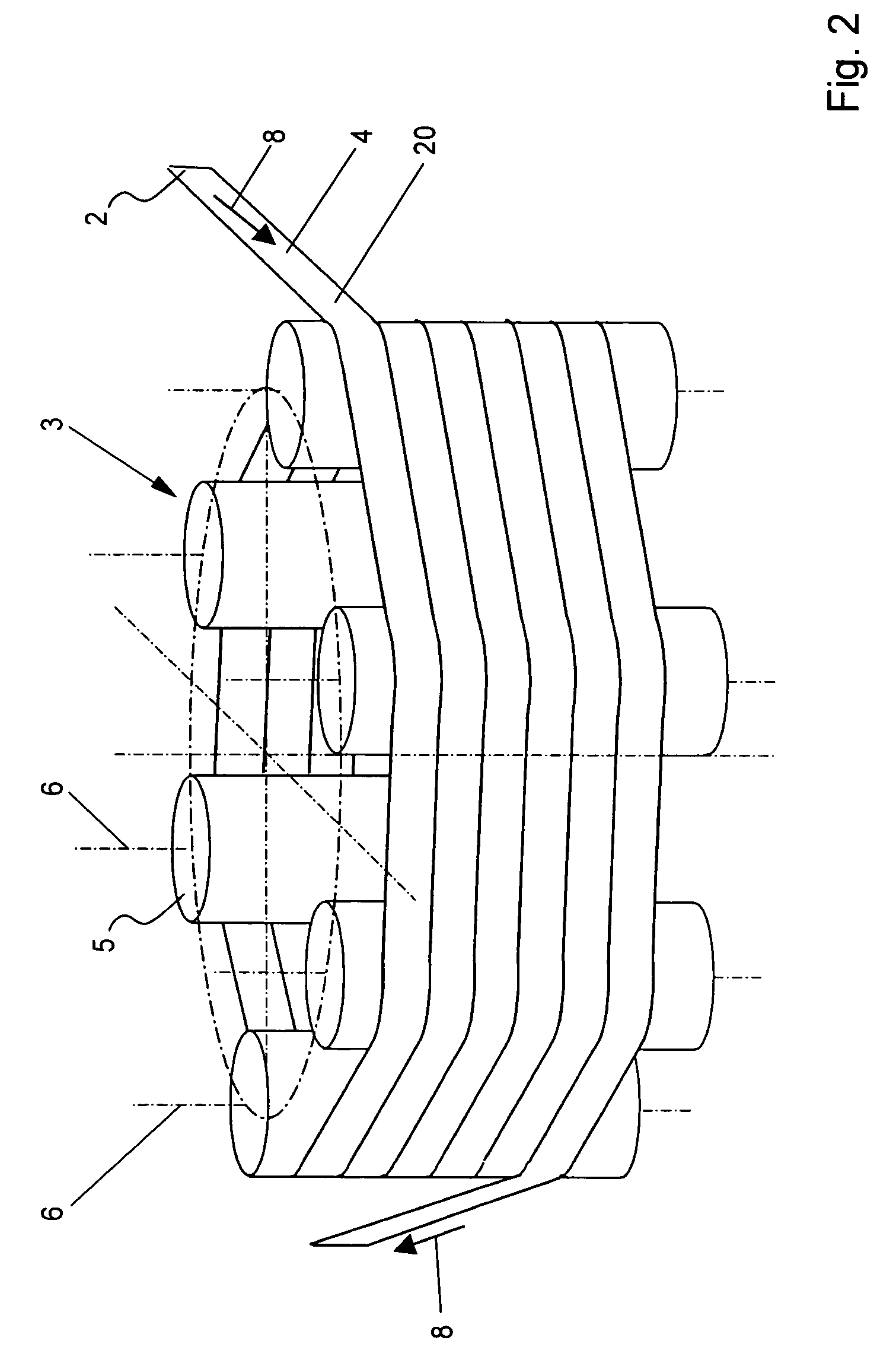
[0051]According to the present invention, a textured thin film 17 of zirconium oxide being stabilized with yttrium oxide (YSC) was deposited on a tape 4 made of stainless CrNi steel. The tape 4 of stainless steel had a length of 10 m, a width of 4 mm and a thickness of 0.1 mm. The surface 20 of the substrate 2 had been polished electrochemically to limit the surface roughness to 4 nm. The tape 4 was wound up about the drum 13 of the apparatus 1 according to FIGS. 3 and 4. The apparatus 1 was then arranged in a vacuum chamber (not illustrated in FIGS. 3 and 4). An ion sputter source was used in the vacuum chamber as the source 9 for atoms, and an ion beam source was used as the source 10 for an energized beam. The diameter of the drum 13 was 1 m. The ion beam source provided an ion beam of argon ions at an angle of incidence of between 51° to 58° with respect to the tape 4. The ion beam source was an ion gun of the “Kaufmann” type with a diameter of 11 cm which delivered particles wi...

example 2

Prior Art; For Reasons of Comparison Only

[0052]For reasons of comparison, a textured layer of zirconium oxide being stabilized with Yttrium oxide (YSC) was produced according to the prior art as disclosed in U.S. Pat. No. 5,432,151, meaning the IBAD method. The conditions of this example were the same ones as in example 1 with the exception of the influence regions of the two sources 9 and 10 on the tape 4 being superimposed. This means that the source 10 in FIG. 3 was rotated about the rotational axis 14 by 180° with respect to the source 9. Furthermore, the influence region of the energized beam 12 on the tape 4 was adapted with respect to its size to the influence region of the source 9 on the tape 4 such that both regions were 80 mm×80 mm. After a time of experimentation of 3.9 hours, one attained a textured thin film 17 having a thickness of 500 nm the biaxial crystal orientation of which was described during an X-ray analysis by a full width at half maximum (phi scan) of 25°. ...

example 3

[0053]Example 3 which was conducted according to the present invention generally was conducted under the same conditions as example 1 with the exception of the time of experimentation being increased to 7.4 hours. The attained textured thin film 17 had a thickness of 850 nm, and its biaxial crystal orientation showed a full width at half maximum (phi scan) during X-ray analysis of 14°.


PUM

PropertyMeasurementUnit
thicknessaaaaaaaaaa
angleaaaaaaaaaa
angleaaaaaaaaaa

Abstract

A method and an apparatus serve to produce thin films having a biaxial crystal orientation. The method includes the steps of: depositing atoms on a substrate, the atoms having a composition corresponding to the thin film to be produced; bombarding the deposited atoms with an energized beam, the energized beam being oriented with respect to the substrate at an angle of a defined range of angles, the step of bombarding substantially taking place during a different time period than the step of depositing; and alternately repeating the step of depositing and the step of bombarding for a plurality of times.

Description

CROSS REFERENCE TO RELATED APPLICATIONS[0001]This application claims priority to co-pending European Patent Application No. EP 05 003 353.9 entitled “Verfahren zur Herstellung biaxial orientierter Dünnschichten und Vorrichtung zur Durchführung dieses Verfahrens”, filed Feb. 17, 2005.FIELD OF THE INVENTION[0002]The present invention generally relates to a method of producing thin films having a biaxial crystal orientation.[0003]The present invention also generally relates to an apparatus for producing thin films having a biaxial crystal orientation.[0004]For example, such thin films or layers having a biaxial crystal orientation are used as buffer layers in superconducting tapes. However, such thin films may also be used for different cases of application.BACKGROUND OF THE INVENTION[0005]A method of producing a thin film having a biaxial crystal orientation is known from U.S. Pat. No. 5,432,151. The known method includes the steps of: depositing atoms on a substrate, the atoms having...

Claims


Application Information

Patent Timeline
Patent Type & Authority Patents(United States)
IPC IPC(8): H05H1/00
CPCC23C14/024C23C14/083C23C14/22H01L39/2461H10N60/0632
Inventor USOSKIN, ALEXANDERKIRCHHOFF, LUTZ
Owner BRUKER HTS
Why Eureka
Try Eureka