
Pin for insertion into a receiving opening in a printed circuit board and method for inserting a pin into a receiving opening in a printed circuit board

a technology of printed circuit boards and receiving openings, which is applied in the direction of fixed connections, manufacturing tools, coupling device connections, etc., can solve the problems of high reliability, reliably low transmission resistance, and the region of printed circuit boards bordering the receiving openings are also subject to high shear forces in the direction, so as to simplify the manufacture of contact parts and facilitate insertion. , the effect of optimal conta

Inactive Publication Date: 2010-11-09
ROBERT BOSCH GMBH
View PDF25 Cites 12 Cited by
  • Summary
  • Abstract
  • Description
  • Claims
  • Application Information

AI Technical Summary

Benefits of technology

The present invention provides a pin with a contact part that can be inserted into a receiving opening of a printed circuit board without applying force and without the risk of breaking away inner layers of the printed circuit board. The contact part is designed to expand transversally to the insertion direction after insertion into the receiving opening, allowing it to be positioned without the need for a sliding fit and to be anchored in the receiving opening with a press fit. The pin includes two adjacently extending leg elements that are separated by a gap or interspace, which allows the contact part to be easily inserted and positioned in the receiving opening. The force required for positioning the pin is introduced through a force introduction surface on one of the leg elements, which is pressed together with an abutment or anvil to deform the leg elements and expand them in the receiving opening. This results in a press fit that securely anchors the contact part in the receiving opening. The invention also provides a method for manufacturing the contact part with the two leg elements joined together in one piece, which simplifies manufacture.

Problems solved by technology

Furthermore, the electrical connections established using the press-in technique are characterized by defect-free contacting and very high reliability, and due to the gas-tight and therefore corrosion-resistant connection between the press-in pins and the printed circuit board have a reliably low transmission resistance over their projected service life.
However, due to the high press-in forces of approximately 70 to 180 N / pin which are necessary for pressing in conventional press-in pins, the regions of the printed circuit board bordering the receiving openings are also subjected to high shear forces in the direction of the press-in forces.
As a result, however, it is possible that a portion of the printed circuit board surface is not able to be used as a circuit surface.
On the other hand, due to high localized mechanical stress on the printed circuit board around the receiving opening, pushing in a press-in pin results in a so-called “jet effect,” a deformation of the printed circuit board bordering the receiving opening caused by shear forces.
For multilayer printed circuit boards, this jet effect entails the risk of conductive metallic inner layers breaking away as the result of extreme tensile stresses.
In addition, there is the risk that a soft metallic sliding layer on the surface of the press-in pins, necessary for pressing in the pin in an operationally reliable manner, may be partially scraped away from the pins when being pressed in from the opening edges of the receiving openings, thus forming chips or flakes which under unfavorable conditions may result in short circuits at other locations on the printed circuit board, and thus, functional failure.

Method used


Image

  • Pin for insertion into a receiving opening in a printed circuit board and method for inserting a pin into a receiving opening in a printed circuit board
  • Pin for insertion into a receiving opening in a printed circuit board and method for inserting a pin into a receiving opening in a printed circuit board

Examples


Embodiment Construction

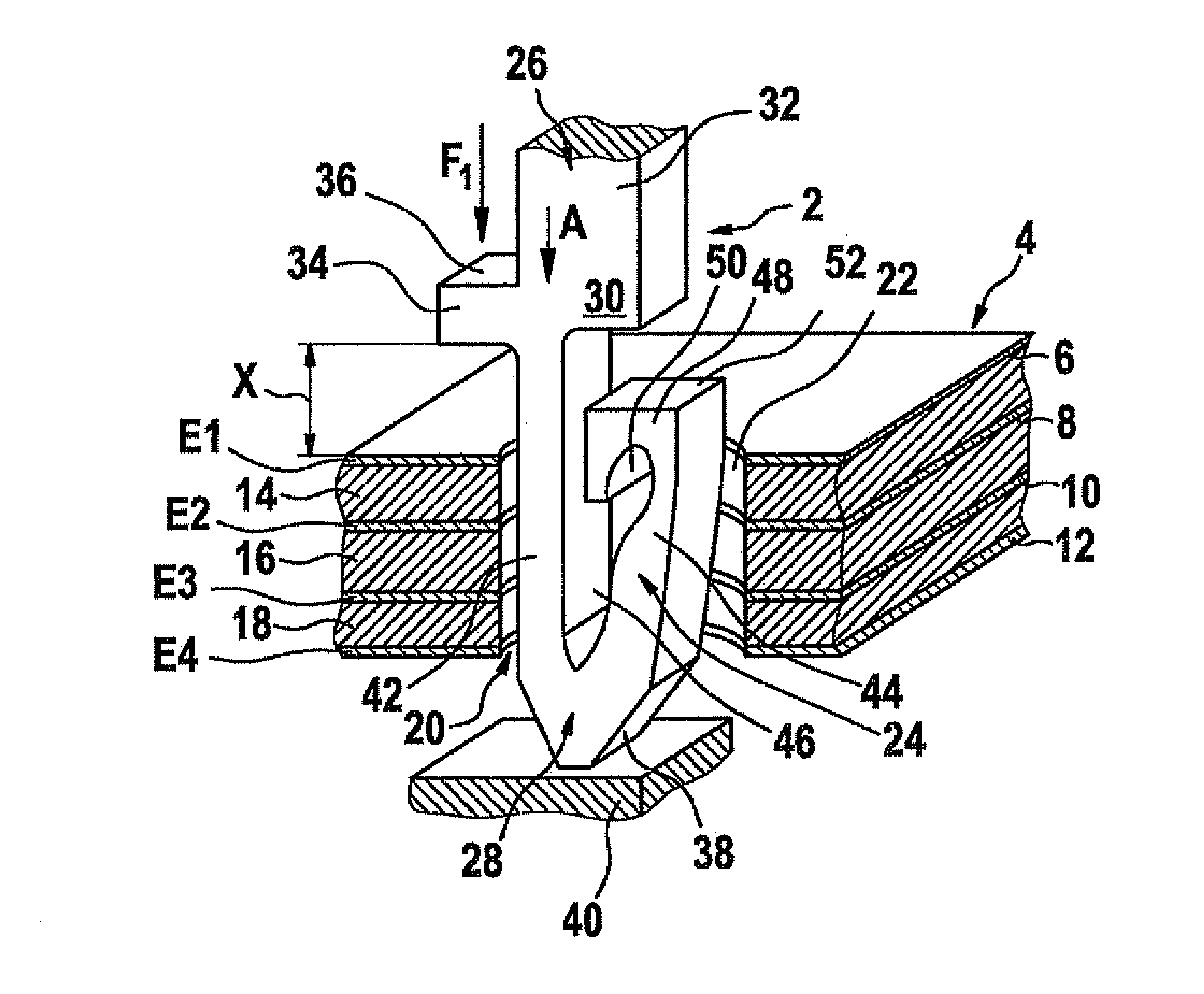
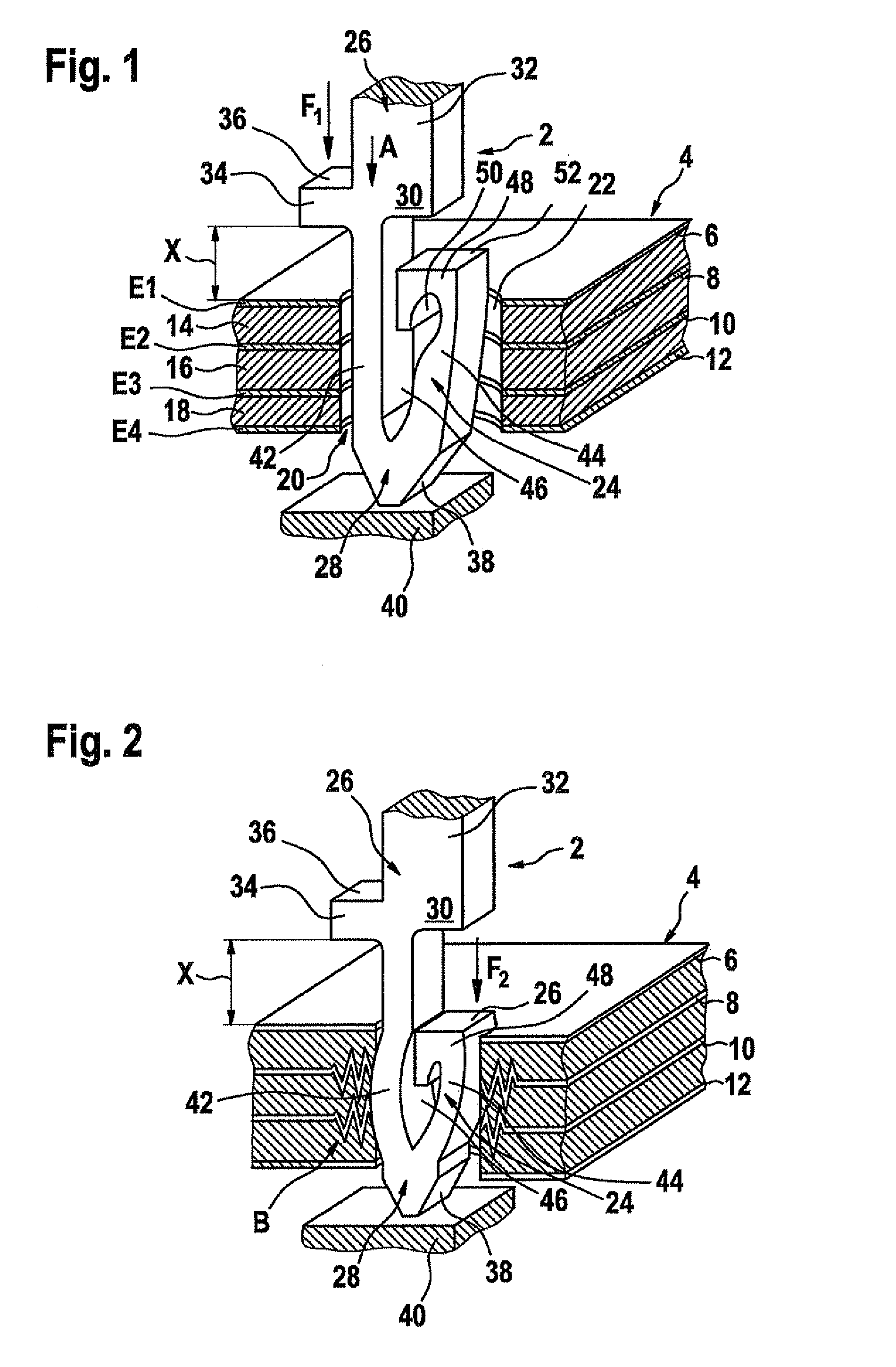
[0017]Pin 2 illustrated in the Figures is used to establish a solder-free electrical connection between a printed circuit board 4 and an electrical or electronic component (not shown) which is to be subsequently mounted on printed circuit board 4, and from which pin 2, optionally together with additional pins, for example as part of a so-called male connector (not shown), projects.

[0018]Multilayer printed circuit board 4 illustrated in the Figures, for example printed circuit board 4 of an airbag control device of a motor vehicle, has a total of four interspaced conductor planes E1, E2, E3, E4, in each of which a printed circuit 6, 8, 10, 12 in the form of printed conductors made of a thin copper layer provided with recesses is situated. Two printed circuits 6 and 12 are located on the oppositely situated broadside surfaces of printed circuit board 4 and in each case form an outer layer, and two printed circuits 8 and 10 are located inside printed circuit board 4 and form two inner ...


PUM

PropertyMeasurementUnit
shear forcesaaaaaaaaaa
deformation forceaaaaaaaaaa
diameteraaaaaaaaaa

Abstract

A pin having a contact part may be inserted into a receiving opening in a printed circuit board and anchored in the receiving opening with a press fit. Also, a method provides for inserting a pin into a receiving opening in a printed circuit board, in which the pin is inserted into the receiving opening from one side of the printed circuit board, and a contact part of the pin is anchored in the receiving opening with a press fit. The contact part is inserted into the receiving opening in a contactless manner or with a sliding fit and is subsequently deformed within the receiving opening by expansion transversally to the insertion direction in order to anchor the contact part in the receiving opening with a press fit.

Description

FIELD OF INVENTION[0001]The present invention relates to a pin, and a method for inserting a pin into a receiving opening in a printed circuit board.BACKGROUND INFORMATION[0002]For situations in automotive technology and other fields in which safe and reliable functioning of control systems is of particular importance, such as for electronic control systems for airbags or other passenger restraint devices, control systems for automatic antilock braking systems (ABS), devices for vehicle dynamics control (ESP), or engine and transmission control systems, the so-called press-in technique, a cold contact method in which one or more projecting press-in pins for the electronic components are inserted with a press fit into complementary receiving openings in the printed circuit board, is being increasingly used for manufacturing high-quality electrical contacts between a printed circuit board and one or more electronic components subsequently installed on the printed circuit board. Howeve...

Claims


Application Information

Patent Timeline
Patent Type & Authority Patents(United States)
IPC IPC(8): H01R13/42H01R12/55H01R12/58
CPCH01R12/585H05K3/308H01R12/7064H01R2201/26H05K2201/1059Y10T29/49945H05K2201/10863H05K2203/1446H05K2201/10856
Inventor GUECKEL, RICHARD
Owner ROBERT BOSCH GMBH
Learn More