Power quad flat no-lead semiconductor die packages with isolated heat sink for high-voltage, high-power applications, systems using the same, and methods of making the same

a technology of semiconductor die packages and heat sinks, applied in semiconductor devices, semiconductor/solid-state device details, electrical apparatuses, etc., can solve problems such as difficult to achieve such goals at the same time, and achieve the effects of excellent voltage isolation, high power dissipation capability, and robust and compact structur

Active Publication Date: 2010-10-19
SEMICON COMPONENTS IND LLC
View PDF21 Cites 12 Cited by
  • Summary
  • Abstract
  • Description
  • Claims
  • Application Information

AI Technical Summary

Benefits of technology

[0005]With this exemplary construction, a robust and compact semiconductor die package for semiconductor power devices can be constructed with high power dissipation capability and excellent voltage isolation for high voltage applications. The electrically conductive layer and the leadframe provide high current connections to the die. The construction also provides dual cooling paths for the device through the top and bottom surfaces of package, and the easy ability of a user to attach an external heat sink to the top surface of the package for additional cooling without the need to use electrically insulating adhesive.

Problems solved by technology

However, achieving such goals simultaneously has been difficult in the prior art.

Method used


Image

  • Power quad flat no-lead semiconductor die packages with isolated heat sink for high-voltage, high-power applications, systems using the same, and methods of making the same
  • Power quad flat no-lead semiconductor die packages with isolated heat sink for high-voltage, high-power applications, systems using the same, and methods of making the same
  • Power quad flat no-lead semiconductor die packages with isolated heat sink for high-voltage, high-power applications, systems using the same, and methods of making the same

Examples


Embodiment Construction

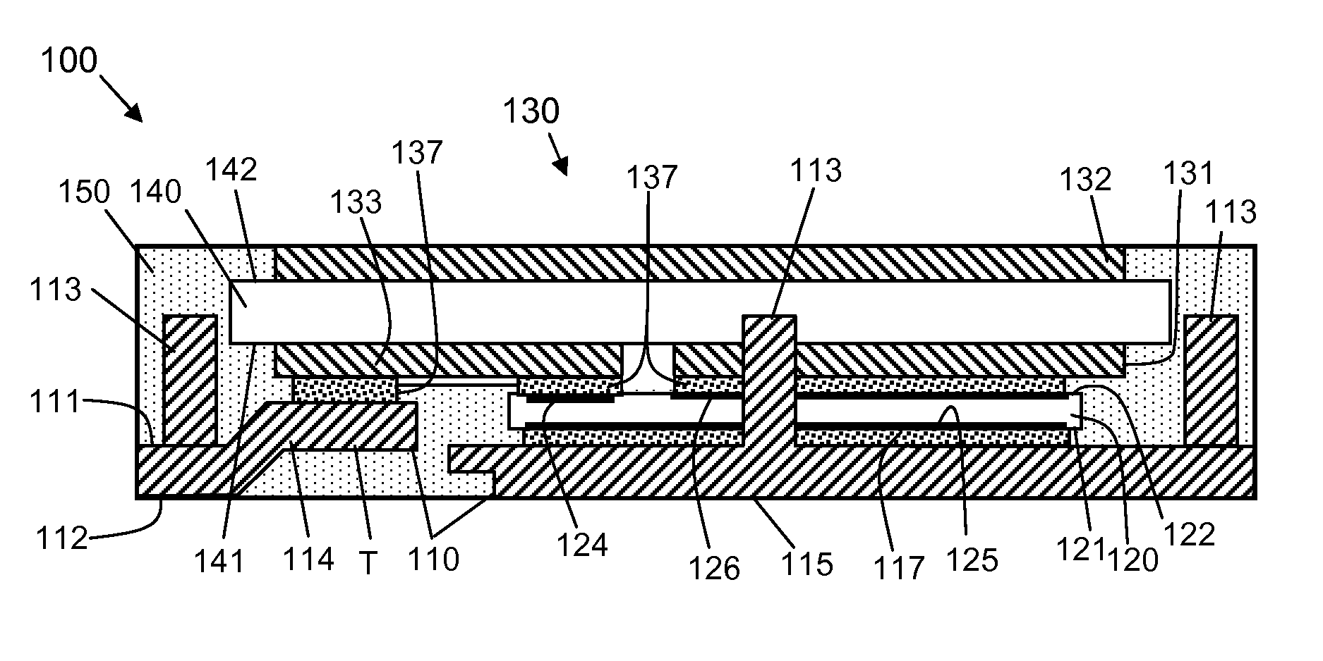
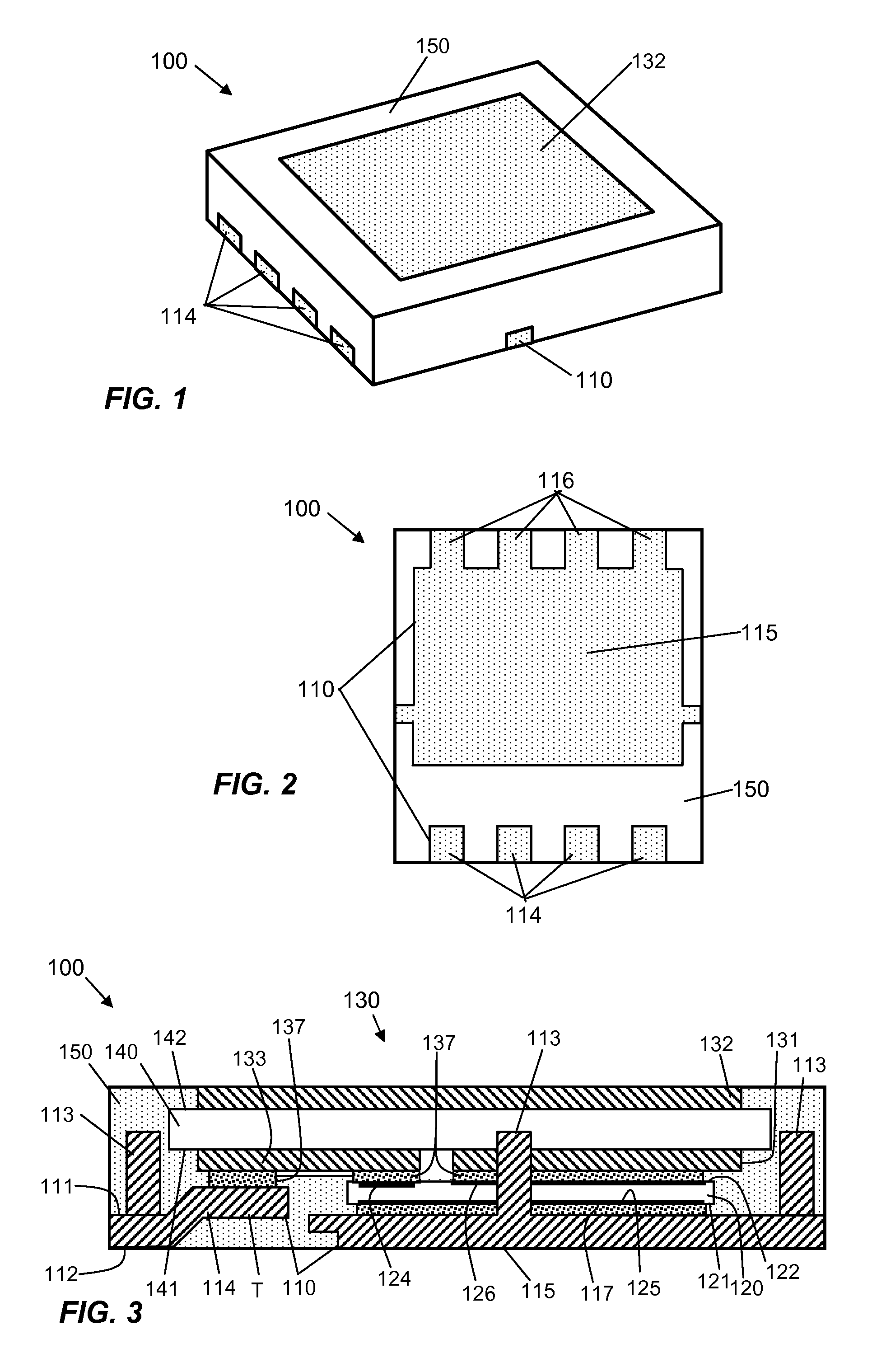
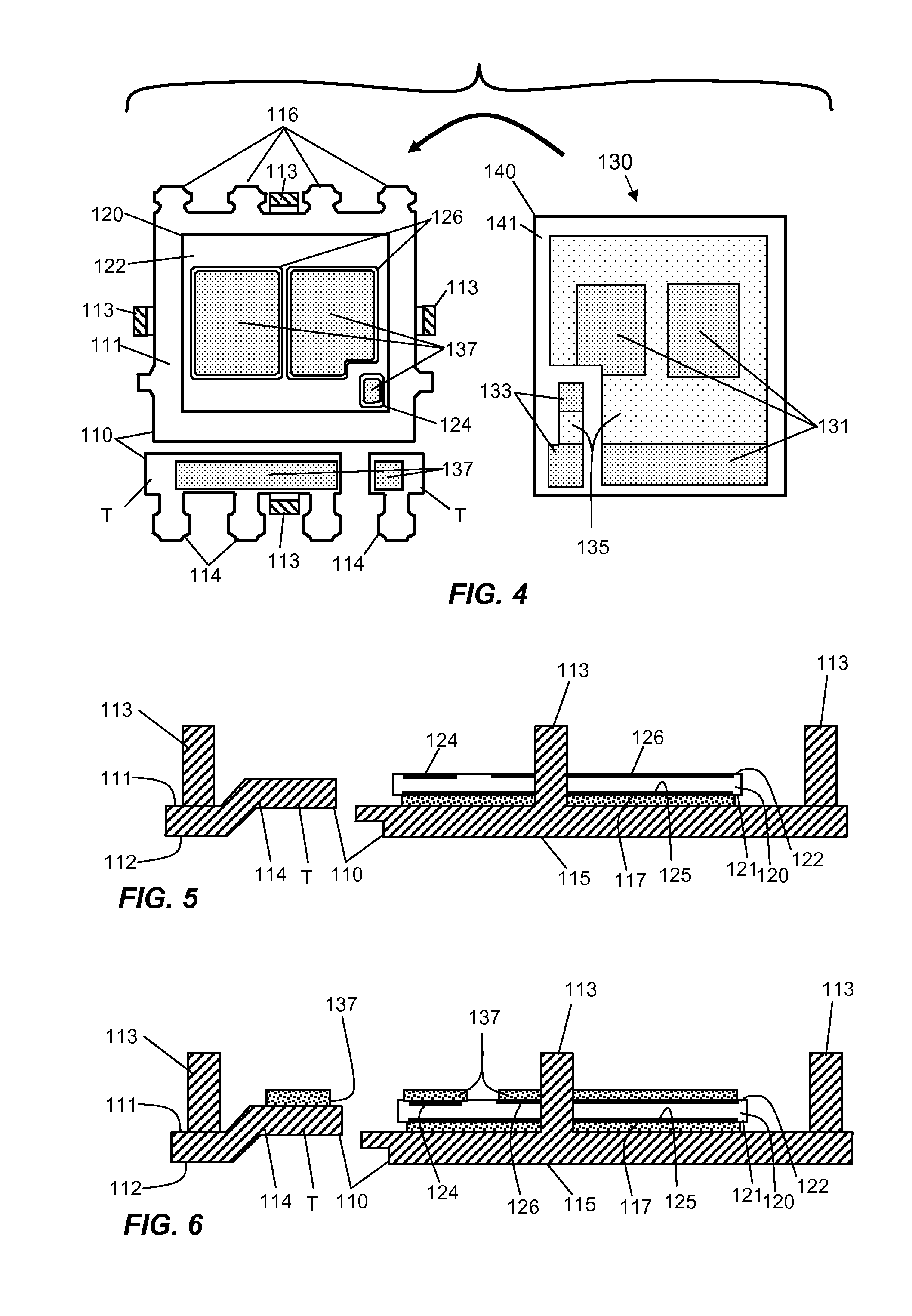
[0013]The present invention will be described more fully hereinafter with reference to the accompanying drawings, in which exemplary embodiments of the invention are shown. This invention may, however, be embodied in different forms and should not be construed as limited to the embodiments set forth herein. Rather, these embodiments are provided so that this disclosure is thorough and complete and fully conveys the scope of the invention to one skilled in the art. In the drawings, the thicknesses of layers and regions may be exaggerated for clarity. The same reference numerals are used to denote the same elements throughout the specification. The elements may have different interrelationships and different positions for different embodiments.

[0014]It will also be understood that when a layer is referred to as being “on” another layer or substrate, it can be directly on the other layer or substrate, or intervening layers may also be present. It will also be understood that when an el...


PUM


Abstract

Disclosed are PQFN semiconductor die packages for high-voltage, high-power applications, systems using the packages, and methods of making the packages. An exemplary package comprises a leadframe, a semiconductor die disposed on the leadframe, and a heat sink member disposed on the semiconductor die and the leadframe and integrated into the molding material of the package. The heat sink member has an electrically insulating substrate with a high breakdown voltage, and one or more conductive layers disposed on a first surface of the substrate that electrically interconnect the semiconductor to one or more leads of the leadframe.

Description

CROSS-REFERENCES TO RELATED APPLICATIONS[0001]Not applicableBACKGROUND OF THE INVENTION[0002]Power semiconductor devices are currently used to switch large amounts of current at moderate voltage levels. They are required to be thermally coupled to relatively large heat sinks, which are bulky and require assembly. Often, there also has to be a layer of electrical insulation between the power device and the heat sink for safety. The layer of electrical insulation may be provided by the package molding, or by a sheet of dielectric material disposed between a metal part of the package (e.g., exposed die paddle) and the heat sink. The first approach has relatively poor thermal conductivity. The second approach makes the assembly of the heat sink more complex.BRIEF SUMMARY OF THE INVENTION[0003]As part of making their invention, the inventors see a need for a low-cost die package for power semiconductor devices that provides high power dissipation capability, high voltage isolation (e.g.,...

Claims


Application Information

Patent Timeline
Patent Type & Authority Patents(United States)
IPC IPC(8): H01L23/34
CPCH01L21/565H01L23/3107H01L23/3735H01L23/4334H01L23/49524H01L23/49562H01L2224/73265H01L2224/32245H01L2224/48091H01L2924/00014H01L2924/18301H01L23/495H01L23/34
Inventor SON, JOON-SEOMANATAD, ROMEL N.JEREZA, ARMAND VINCENT
Owner SEMICON COMPONENTS IND LLC
Why Eureka
Try Eureka