Method of controlling film stress in MEMS devices

a technology of micro-electromechanical systems and film stress, which is applied in the direction of micro-structural devices, micro-gyroscopes, micro-actuators, etc., can solve the problems of affecting the interaction of the manufacturing process and the manufacturing of micro-electromechanical systems such as micro-gyroscopes, which integrate very sensitive moving mechanical parts

Active Publication Date: 2010-09-21
TELEDYNE DIGITAL IMAGING INC
View PDF11 Cites 0 Cited by
  • Summary
  • Abstract
  • Description
  • Claims
  • Application Information

AI Technical Summary

Benefits of technology

[0025]The present invention adopts a novel approach that allows one to vary the mechanical stress obtained after annealing the deposited Si layer to be either tensile or compressive. Impressive mechanical stress uniformities are also demonstrated with this approach. Such a process therefore presents a tremendous advantage in terms of the potential for integration in various Micro-Electro-Mechanical Systems (MEMS) or Nano-Electro-Mechanical Systems (NEMS) as one can choose the nature of the mechanical stress itself as well as the desired stress in addition to adjusting the stress gradient to the required values.
[0027]It has been widely believed in the industry that the nitrogen (N2) carrier gas used along with phosphine (PH3) did not have any impact on the film properties of the in-situ doped poly-Si or in-situ doped amorphous Si. The present invention however clearly demonstrates that, contrary to prior art belief, changing this N2 carrier gas, although believed to be inert in the LPCVD reaction taking place, by an Ar carrier gas drastically modifies the film properties and therefore, opens a whole window of new possibilities and potential for device fabrication.

Problems solved by technology

The manufacture of Micro-Electro-Mechanical Systems (MEMS) such as micro-gyroscopes, micro-accelerometers, RF micro-resonators, micro-mirrors, micro-motors, micro-actuators and other such micro-devices integrating very sensitive moving mechanical parts poses some very serious challenges because they must meet a number of stringent requirements.
The integration of all the materials together may cause some detrimental interactions due to the thermal budget and the subsequent annealing steps that could thus affect the layers previously deposited / annealed and therefore modify the film stress and stress gradient values along the processing of the devices.vi.
It may also be required to combine annealed with non-annealed structures or to combine doped with undoped layers in order to achieve the desired stress values which in turn increases the manufacturing costs and / or complexity.
However, such film is not conductive and displays a 2 μm deflection over a 310-μm long beam.
Despite the high potential of such a deposition method, this film presents severe drawbacks due to the stress gradient and the film resistivity.
In addition, this material developed by Case Western Reserve University does not allow one to deposit a film with the exact stress level desired.
Nevertheless, this film does not provide one a good control of the stress.
Although depositing a film in-situ doped with As and P leads to a low-stress layer, it does not allow one to easily select the desired stress.
In this case however, the film resistivity would not be uniform throughout the entire thickness of the film therefore requiring an annealing step which would then annihilate the impact of the multilayer process and would thus lead to an undesired stress value.

Method used


Image

  • Method of controlling film stress in MEMS devices
  • Method of controlling film stress in MEMS devices
  • Method of controlling film stress in MEMS devices

Examples


Embodiment Construction

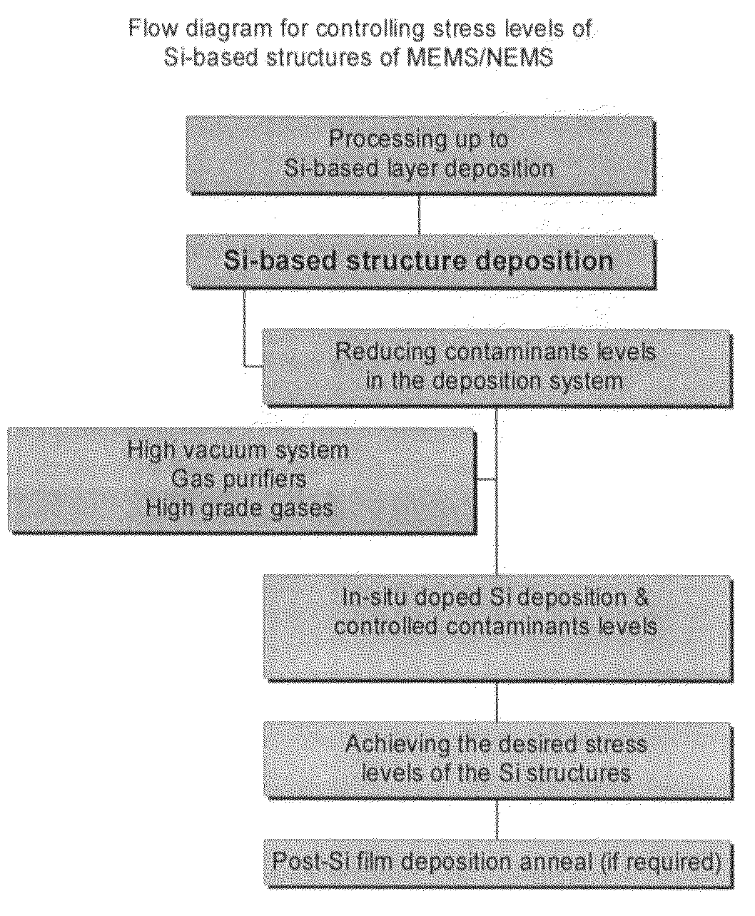
[0078]In order to assist the reader in understanding the invention, a detailed discussion of the underlying materials science will be undertaken.

Impact of a Si Film Anneal on Film Properties

[0079]The impact of an anneal performed at 1100° C. on the film resistivity, mechanical stress and stress gradient properties can be analyzed by capping the deposited Si film with an oxide layer in order to prevent the loss of dopants. In addition, this allows one to have a “barrier” therefore preventing the contamination of the Si-based film by the annealing ambient. In that case, the Si film deposited is an in-situ doped amorphous Si film. The dopant used is phosphorus while nitrogen is used as the carrier gas for phosphine unless specified otherwise. Film resistivity

[0080]The resistivity results achieved for various film thickness before and after annealing the Si layer are shown in FIG. 7. This figure demonstrates that the annealing step significantly lowers the film resistivity. Prior to ann...


PUM

PropertyMeasurementUnit
temperatureaaaaaaaaaa
partial pressureaaaaaaaaaa

Abstract

A structural film, typically of silicon, in MEMS or NEMS devices is fabricated by depositing the film in the presence of a gas other than nitrogen, and preferably argon as the carrier gas.

Description

FIELD OF THE INVENTION[0001]This invention relates to the manufacture of Micro Electromechanical Systems (MEMS) or NEMS (Nano Electromechanical Systems) devices, and in particular to a method of controlling film stress in the manufacture of such devices, and in particular silicon film stress.BACKGROUND OF THE INVENTION[0002]The manufacture of Micro-Electro-Mechanical Systems (MEMS) such as micro-gyroscopes, micro-accelerometers, RF micro-resonators, micro-mirrors, micro-motors, micro-actuators and other such micro-devices integrating very sensitive moving mechanical parts poses some very serious challenges because they must meet a number of stringent requirements. Specifically:[0003]i. These very sensitive mechanical parts are typically made of silicon, (polysilicon or silicon-germanium).[0004]ii. Such mechanical parts need to display either low or specific stress values and low or specific stress gradient properties which is typically achieved during a stress / stress-gradient relief...

Claims


Application Information

Patent Timeline
Patent Type & Authority Patents(United States)
IPC IPC(8): C23C16/24
CPCB81C1/00666C23C16/24C23C16/56B81C2201/017
Inventor FORTIN, VINCENTOUELLET, LUC
Owner TELEDYNE DIGITAL IMAGING INC
Why Eureka
Try Eureka