
Method and apparatus for producing interferometric lithography patterns with circular symmetry

a technology of circular symmetry and lithography, which is applied in the direction of semiconductor/solid-state device testing/measurement, instruments, polarising elements, etc., can solve the problems of not being suitable for producing the desired wave of conventional optical systems, such as lenses machined with spherical radii of curvature, and achieve the desired wave

Active Publication Date: 2010-09-14
STC UNM
View PDF2 Cites 11 Cited by
  • Summary
  • Abstract
  • Description
  • Claims
  • Application Information

AI Technical Summary

Benefits of technology

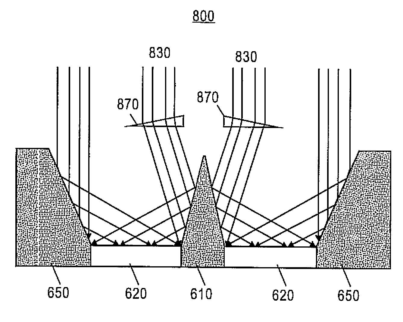
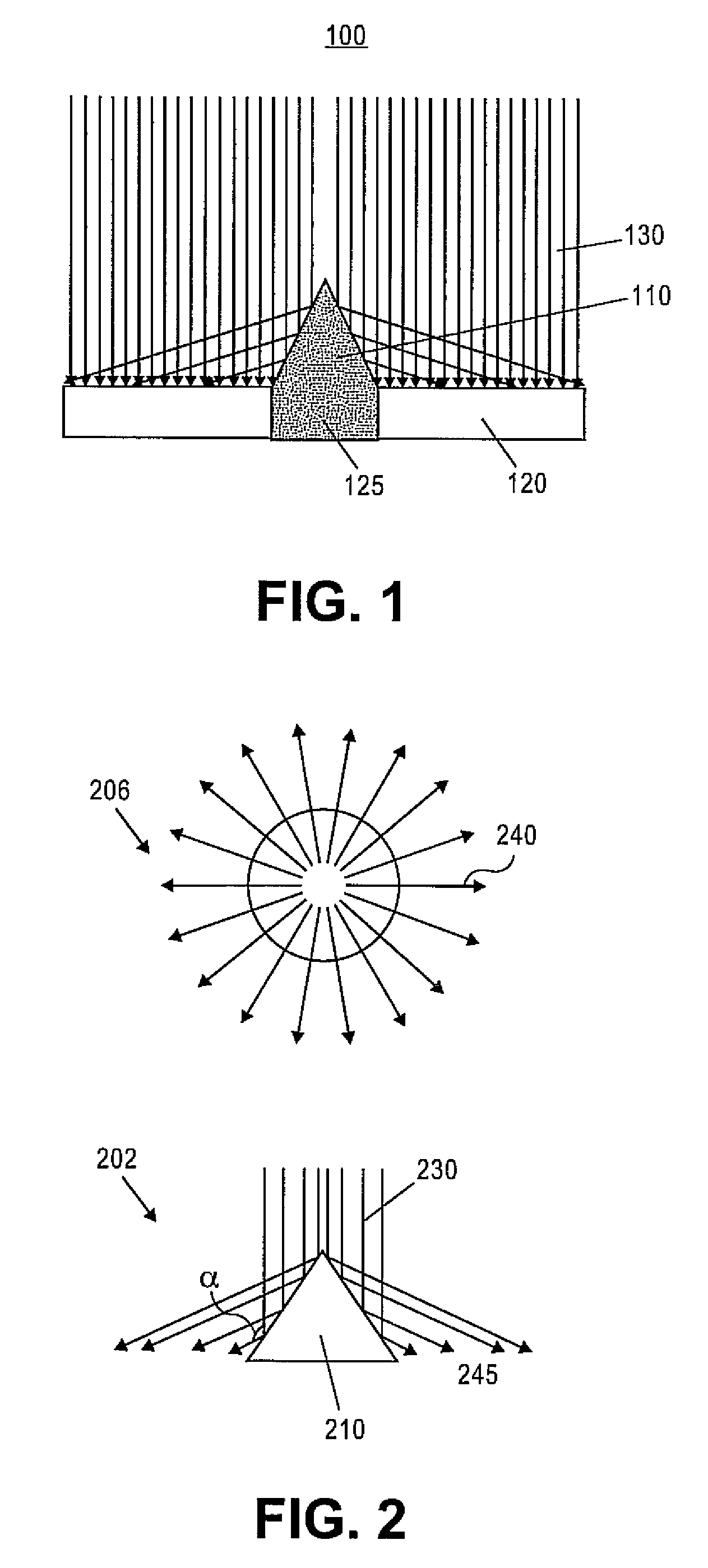
The present patent teaches an optical system and a method for creating an interference pattern. The system includes an axicon optic that transforms a plane wave into a radial symmetric wave with a constant angle of incidence onto a photoresist layer. The transformed wave is then interfered with a second portion of the plane wave to create a periodic spatially-varying intensity pattern with circular symmetry. The method involves using the optical system to create the interference pattern, which can be useful in various applications such as semiconductor device manufacturing.

Problems solved by technology

Conventional optical systems (such as lens machined with spherical radii of curvature), however, are not suitable for production of these desired waves.

Method used


Image

  • Method and apparatus for producing interferometric lithography patterns with circular symmetry
  • Method and apparatus for producing interferometric lithography patterns with circular symmetry
  • Method and apparatus for producing interferometric lithography patterns with circular symmetry

Examples


Embodiment Construction

[0002]1. Field of the Invention

[0003]This invention relates generally to microelectronic circuits and, more particularly, to methods and apparatus for producing semiconductor patterns with circular symmetry.

[0004]2. Background of the Invention

[0005]Interferometric lithography (IL) is emerging as a powerful technique for the fabrication of large areas of nanostructures. For example, an optical geometry having two-plane-wave interference is commonly used to produce one-dimensional (i.e., 1D) nanopatterns (e.g., gratings). 2D patterns are obtained by repeating the exposure step with the wafer rotated 90° (e.g., square pattern) or 60° (e.g., hexagonal pattern). More complex patterns are obtained by using other angular rotations, variations in the pitch for a single exposure, and / or additional exposures.

[0006]Nanopatterns having an overall circular symmetry are desired in many applications such as modern memory devices. In this case, an optical system is required to produce a wave with a...


PUM

PropertyMeasurementUnit
opening angleaaaaaaaaaa
wavelengthsaaaaaaaaaa

Abstract

Exemplary embodiments provide optical systems and methods for producing interferometric lithography (IL) patterns with circular symmetry for applications such as memory devices including CD ROMs, DVDs, magnetic hard disk storage, and the like. Specifically, one or more axicon optics can be configured in the optical systems for IL patterning processes to form a uniform set of rings with constant increment in all directions in a developed photoresist. In an exemplary embodiment, the optical system can transform a first portion of a plane wave into a radial symmetric wave with a constant angle of incidence onto a photoresist plane of a wafer. This radial symmetric wave can then interfere with a second portion of the plane wave incident but with a different angle of incidence to produce a periodic spatially-varying intensity pattern with circular symmetry.

Description

RELATED APPLICATIONS[0001]This application claims priority from U.S. Provisional Patent Application Ser. No. 60 / 794,142, filed Apr. 24, 2006, which is hereby incorporated by reference in its entirety.DESCRIPTION OF THE INVENTION[0002]1. Field of the Invention[0003]This invention relates generally to microelectronic circuits and, more particularly, to methods and apparatus for producing semiconductor patterns with circular symmetry.[0004]2. Background of the Invention[0005]Interferometric lithography (IL) is emerging as a powerful technique for the fabrication of large areas of nanostructures. For example, an optical geometry having two-plane-wave interference is commonly used to produce one-dimensional (i.e., 1D) nanopatterns (e.g., gratings). 2D patterns are obtained by repeating the exposure step with the wafer rotated 90° (e.g., square pattern) or 60° (e.g., hexagonal pattern). More complex patterns are obtained by using other angular rotations, variations in the pitch for a sing...

Claims


Application Information

Patent Timeline
Patent Type & Authority Patents(United States)
IPC IPC(8): G03C5/00G02B5/30
CPCG03F7/70408
Inventor BRUECK, STEVEN R. J.
Owner STC UNM
Learn More