
Memory cell array latchup prevention

a memory cell array and latchup prevention technology, applied in the field of integrated circuits, can solve the problems of cmos circuits that are not suitable for switching, scr enters a low impedance state, and the junctions of circuit bipolar transistors to become forward-biased, so as to improve the reliability of the device and improve the reliability of the cmos circui

Active Publication Date: 2010-08-10
INFINEON TECH LLC
View PDF81 Cites 17 Cited by
  • Summary
  • Abstract
  • Description
  • Claims
  • Application Information

AI Technical Summary

Benefits of technology

[0010]The problems outlined above may be in large part addressed by a CMOS circuit having one or more current-limiting devices arranged along a power-supply bus and / or a ground bus of the circuit which are configured to prevent latch up within the circuit. More specifically, the one or more current-limiting devices may be configured to maintain a junction of a parasitic pnpn diode structure within the circuit as reverse-biased such that latch up within the circuit may be prevented. More specifically, the one or more current-limiting devices may be configured to prevent end junctions of a parasitic pnpn diode structure from achieving forward biases sufficient or strong enough to forward bias a middle junction of the parasitic pnpn diode structure. A current limiting device arranged along the power-supply bus may include a resistor or a p-channel field-effect transistor pass gate. Alternatively, a current limiting device arranged along the ground bus may include a resistor or an n-channel field-effect transistor pass gate. In either case, the one or more current-limiting devices may be specifically configured to prevent latch up caused by high energy radiation on the circuit. In particular, one or more current-limiting devices may be configured to prevent latch up caused by alpha particles and / or cosmic rays. In addition or alternatively, the one or more current-limiting devices may be configured to prevent latch up caused by current injecting defects within the circuit. Furthermore, the one or more current-limiting devices may be configured to eliminate single event latch up caused by excessive substrate current to the CMOS circuit.
[0013]There may be several advantages for providing the CMOS circuit and method described herein. In particular, a CMOS circuit may be fabricated which is immune or free from latch up. As a result, the reliability of CMOS circuits may be improved. In addition, the inclusion of one or more current-limiting devices along the power-supply bus of a CMOS circuit does not affect write and read operations of the circuit and, therefore, circuit simulation models of circuits do not have change with the incorporation of current-limiting devices. Moreover, the formation of current-limiting devices is not significantly sensitive to fabrications variations. Consequently, incorporating current-limiting devices within a CMOS circuit does not cause a significant variance in the functionality of the device. Another advantage of the inclusion of one or more current-limiting devices with a CMOS circuit is that single even latch up (SEL) caused by excessive substrate current may be completely eliminated, thereby improving the reliability of the device.

Problems solved by technology

A disadvantage of forming an SCR within a CMOS circuit is that it allows a low-resistance path between power supply buses to form, which in turn allows high amounts of current to flow through the circuit.
In particular, internal voltages across the anode and cathode of an SCR which exceed a breakover or trigger voltage can cause junctions within the bipolar transistors of the circuit to become forward-biased.
As a result, the SCR enters into a low impedance state with the possibility of a resultant high current.
As a consequence, the memory cells of the circuit may be restricted from switching and may lose their data.
As a consequence, cell size is undesirably increased and the objective to increase memory cell density is hindered.
The formation of low resistance well regions, however, induces higher junction capacitance, which may undesirably increase the threshold voltage at which devices operate.
Higher threshold voltages lead to decreased circuit speeds, which is contrary to the industry objective to increase processing speeds within circuits.
Moreover, the formation of low resistance well regions does not completely eliminate the formation of latch up.
Misplacement of well regions may adversely affect the functionality of the device and, in some cases, cause the device to malfunction.
In addition, the diffusion of dopants both vertically and horizontally can vary with the temperature, affecting the efficacy of low resistance wells.

Method used


Image

  • Memory cell array latchup prevention
  • Memory cell array latchup prevention
  • Memory cell array latchup prevention

Examples


Embodiment Construction

[0024]Turning to the drawings, exemplary embodiments of CMOS circuits having current limiting devices arranged along power-supply buses and / or ground buses are illustrated. In particular, FIG. 1a illustrates resistor RL formed along power-supply bus 12 of CMOS circuit 10. FIG. 1b illustrates p-channel pass gate transistor 26 formed along power-supply bus 22 of CMOS circuit 20. CMOS circuit 30 is shown in FIG. 2 having current-limiting device 36 along ground bus 34 and CMOS circuit 40 shown in FIG. 3 includes current-limiting devices 46 and 48 arranged along power-supply bus 42 and ground bus 44, respectively. Each of the circuits is described in more detail below, particularly in reference to the arrangement and type of current-limiting devices included therein. In addition to the current-limiting devices, the CMOS circuits depicted in FIGS. 1a-3 include parasitic resistances Rw and Rs, respectively referring to parasitic resistances of the well regions and substrate used to form co...


PUM


Abstract

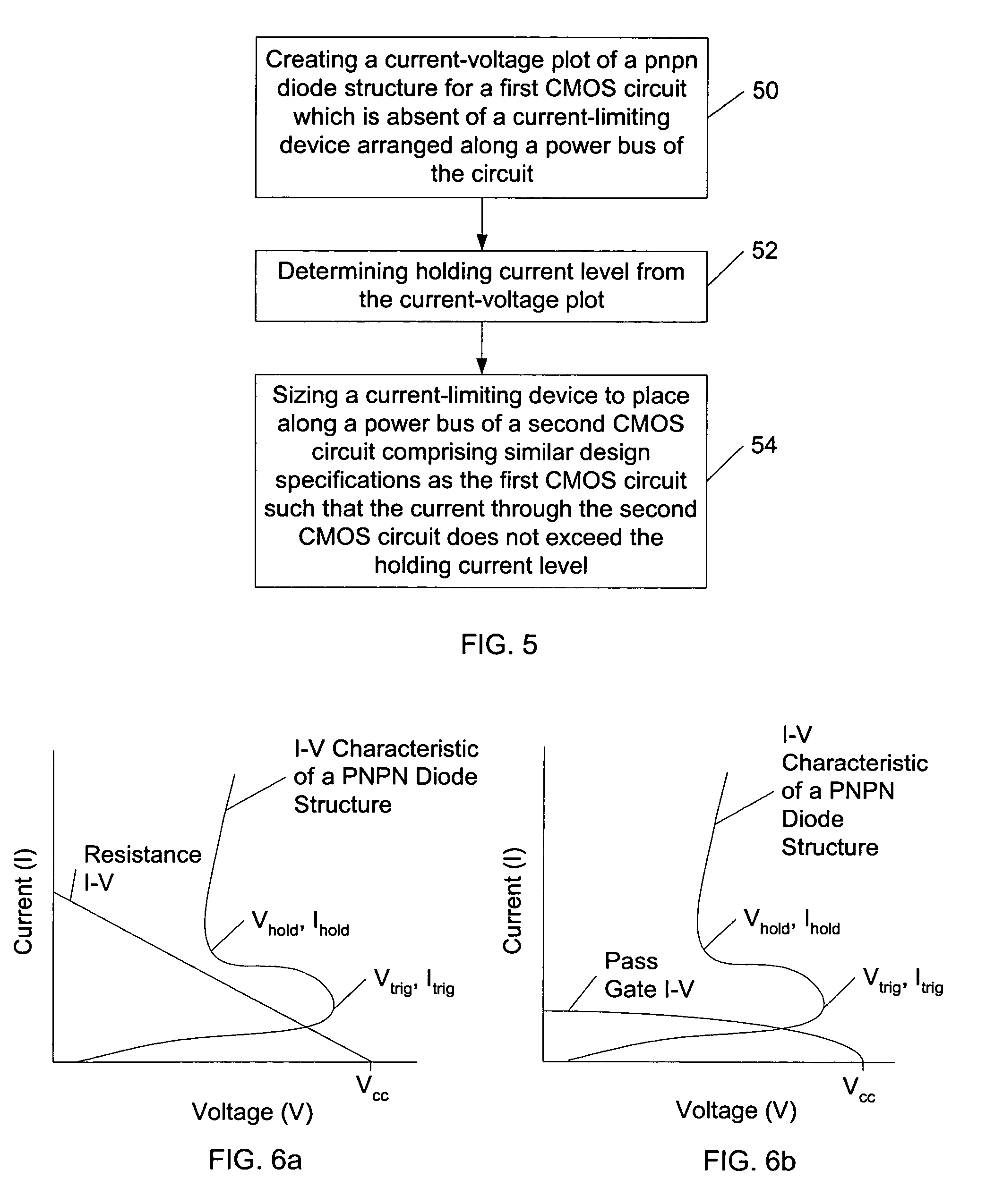
A complementary field-effect (CMOS) circuit is provided which includes a current-limiting device arranged along a power-supply bus or a ground bus of the circuit. The current-limiting device is configured to prevent latch up of the CMOS circuit. More specifically, the current-limiting device is configured to maintain a junction of the parasitic pnpn diode structure as reverse-biased. A method is also provided which includes creating a current-voltage plot of a pnpn diode arranged within a first CMOS circuit which is absent of a current-limiting device arranged along a power bus of the circuit. In addition, the method includes determining a holding current level from the current-voltage plot and sizing a current-limiting device to place along a power bus of a second CMOS circuit comprising similar design specifications as the first CMOS circuit such that the current through the second CMOS circuit does not exceed the holding current level.

Description

BACKGROUND OF THE INVENTION[0001]1. Field of the Invention[0002]This invention relates to integrated circuits and, more specifically, complementary metal oxide semiconductor (CMOS) memory circuits that are configured to be free or immune from latch up.[0003]2. Description of the Related Art[0004]The following descriptions and examples are given as background information only.[0005]Integrated circuit semiconductor devices using CMOS technology inherently contain parasitic bipolar pnp and npn transistors in the structure of p-channel metal oxide semiconductor (PMOS) and n-channel metal oxide semiconductor (NMOS) devices. For example, in a structure of a n-well CMOS circuit, a parasitic pnp bipolar transistor may be formed when a source / drain region of a PMOS device acts as an emitter, the n-well of the PMOS device acts as a base, and a p-type doped substrate acts as the collector. In addition, a parasitic npn bipolar transistor may be formed when a source / drain region of the NMOS devi...

Claims


Application Information

Patent Timeline
Patent Type & Authority Patents(United States)
IPC IPC(8): G11C7/02G11C5/14G11C11/34H01L27/092H02H9/02
CPCG11C5/14G11C11/417H02H9/025H01L27/0921G11C7/00
Inventor KAPRE, RAVINDRA M.SHARIFZADEH, SHAHIN
Owner INFINEON TECH LLC
Learn More