Integrated SiGe NMOS and PMOS transistors

a technology of integrated bicmos and sige, which is applied in the direction of semiconductor devices, electrical devices, transistors, etc., can solve the problems of complex fabrication process

Active Publication Date: 2010-08-10
TEXAS INSTR INC
View PDF77 Cites 3 Cited by
  • Summary
  • Abstract
  • Description
  • Claims
  • Application Information

AI Technical Summary

Benefits of technology

[0014]In another aspect, the invention provides a BiCMOS integrated circuit including bipolar transistors and CMOS transistors on a substrate, the circuit comprising an epitaxial layer which includes a dopant and which forms a channel region of a MOS transistor and a base region of a bipolar transistor. In an implementation, the epitaxial layer (28) has a first sublayer of silicon; a first sublayer of silicon-germanium on top

Problems solved by technology

Forming so-called BiCMOS circuits demands a complicated fabrication process with many steps, as fabrication steps performing base,

Method used


Image

  • Integrated SiGe NMOS and PMOS transistors
  • Integrated SiGe NMOS and PMOS transistors
  • Integrated SiGe NMOS and PMOS transistors

Examples


Embodiment Construction

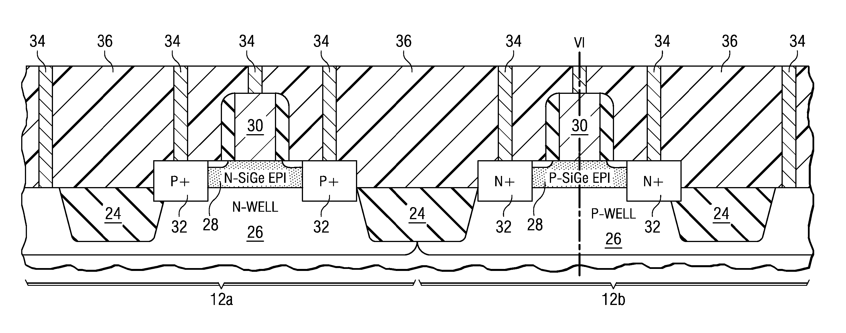
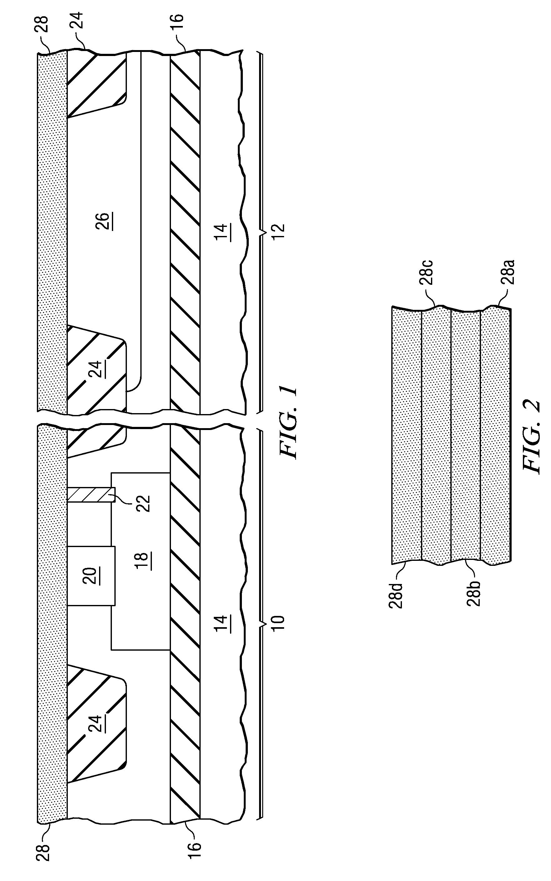
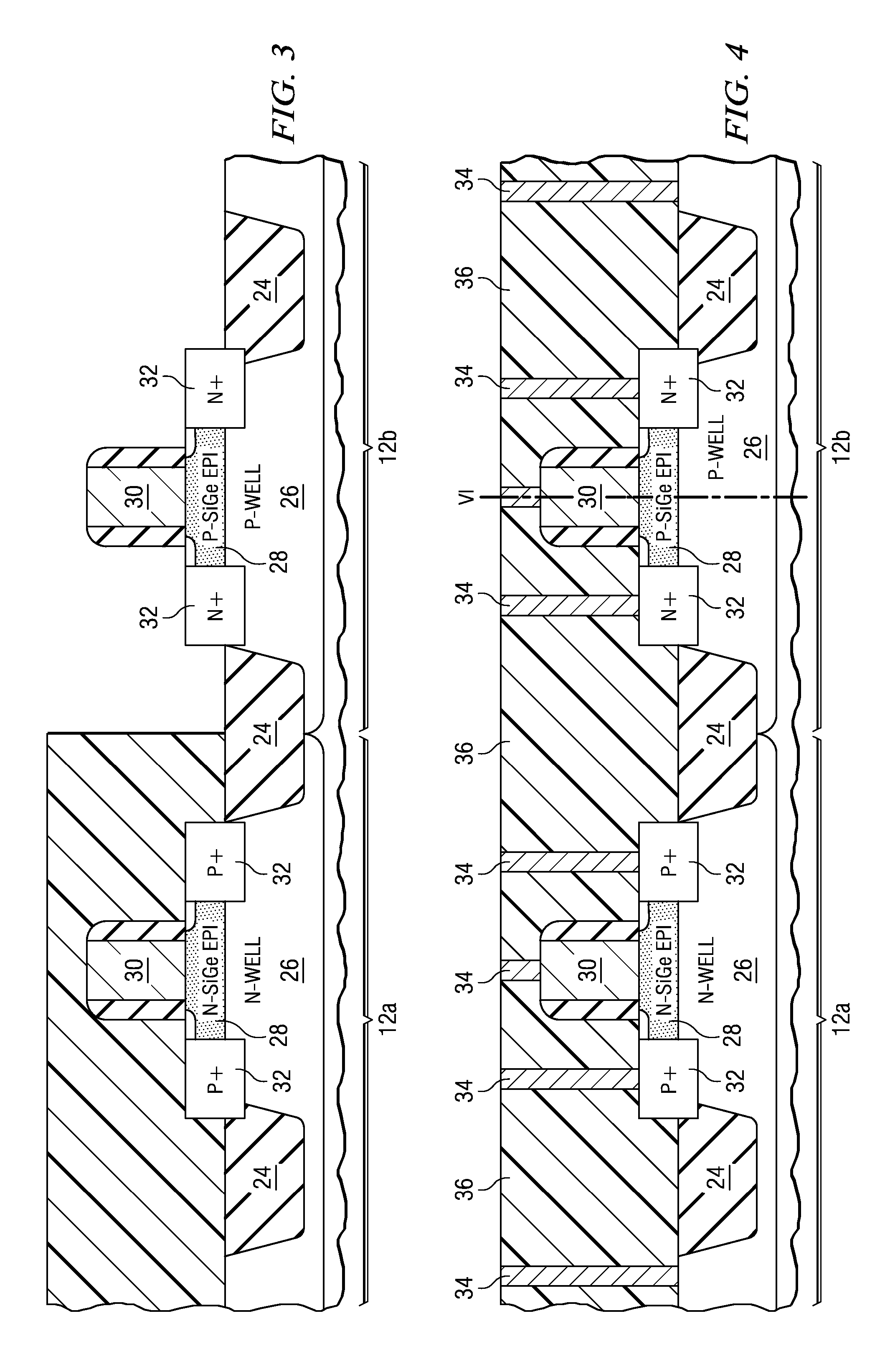
[0021]FIGS. 1 to 5 are schematic views showing structures relevant to the described example embodiments the invention. Those skilled in the art will appreciate that other steps and features of various kinds will also be present. The drawings and, in particular, the relative thicknesses of the illustrated sublayers, are not to scale.

[0022]In FIG. 1, the sectional view through a wafer shows on the left hand side the first structures formed for a bipolar transistor 10 and on the right hand side the first structures formed for a field effect transistor 12. The two transistors 10 and 12 may be neighboring on a BiCMOS circuit or they may be separated by other structures. This fact is indicated by the dashed lines in the middle of FIG. 1. On a substrate 14, which may be a silicon wafer, a buried oxide layer 16 is formed of silicon dioxide for example and used for electrically insulating the overlying layers. For the bipolar transistor 10 a buried layer 18 is formed, which is doped with a h...


PUM


Abstract

A method of fabricating an integrated BiCMOS circuit is provided, the circuit including bipolar transistors 10 and CMOS transistors 12 on a substrate. The method comprises the step of forming an epitaxial layer 28 to form a channel region of a MOS transistor and a base region of a bipolar transistor. Growing of the epitaxial layer includes growing a first sublayer of silicon 28a, a first sublayer of silicon-germanium 28b onto the first sublayer of silicon, a second sublayer of silicon 28c onto the first sublayer of silicon-germanium, and a second sublayer of silicon-germanium 28d onto the second sublayer of silicon. Furthermore, an integrated BiCMOS circuit is provided, which includes an epitaxial layer 28 as described above.

Description

[0001]This application claims priority under 35 U.S.C. 119 from German Application No. DE 10 2006 028 543.3 filed Jun. 21, 2006, and from U.S. Provisional Application No. 60 / 882,367 filed Dec. 28, 2006, the entireties of both of which are incorporated herein by reference.BACKGROUND[0002]The invention relates to a method of fabricating an integrated BiCMOS circuit including bipolar transistors and CMOS transistors on a substrate. In particular, the invention relates to a method comprising the step of forming an epitaxial layer including a silicon germanium sublayer. The invention further relates to an integrated BiCMOS circuit comprising an epitaxial layer with a silicon-germanium sublayer.[0003]It is known to integrate bipolar devices with MOSFET devices on a substrate. Forming so-called BiCMOS circuits demands a complicated fabrication process with many steps, as fabrication steps performing base, emitter and collector of a bipolar transistor differ from fabrication steps for formi...

Claims


Application Information

Patent Timeline
IPC IPC(8): H01L21/8238
CPCH01L21/823807H01L21/8249H01L27/0623
Inventor JUMPERTZ, REINERSCHIMPF, KLAUS
Owner TEXAS INSTR INC
Why Eureka
Try Eureka