Method of forming gate pattern of flash memory device including over etch with argon
a technology of flash memory and gate pattern, which is applied in the direction of semiconductor devices, basic electric elements, electrical equipment, etc., can solve the problems of reducing electrical properties, slow operation of the device, and bowing profile, so as to reduce the bowing profile, improve the anisotropic etch characteristic of plasma, and reduce the over etch
- Summary
- Abstract
- Description
- Claims
- Application Information
AI Technical Summary
Benefits of technology
Problems solved by technology
Method used
Image

Examples
Embodiment Construction
[0015]Preferred embodiments of the present invention will be described with reference to the accompanying drawings. These embodiments are used only for illustrative purpose, the invention is not limited thereto.
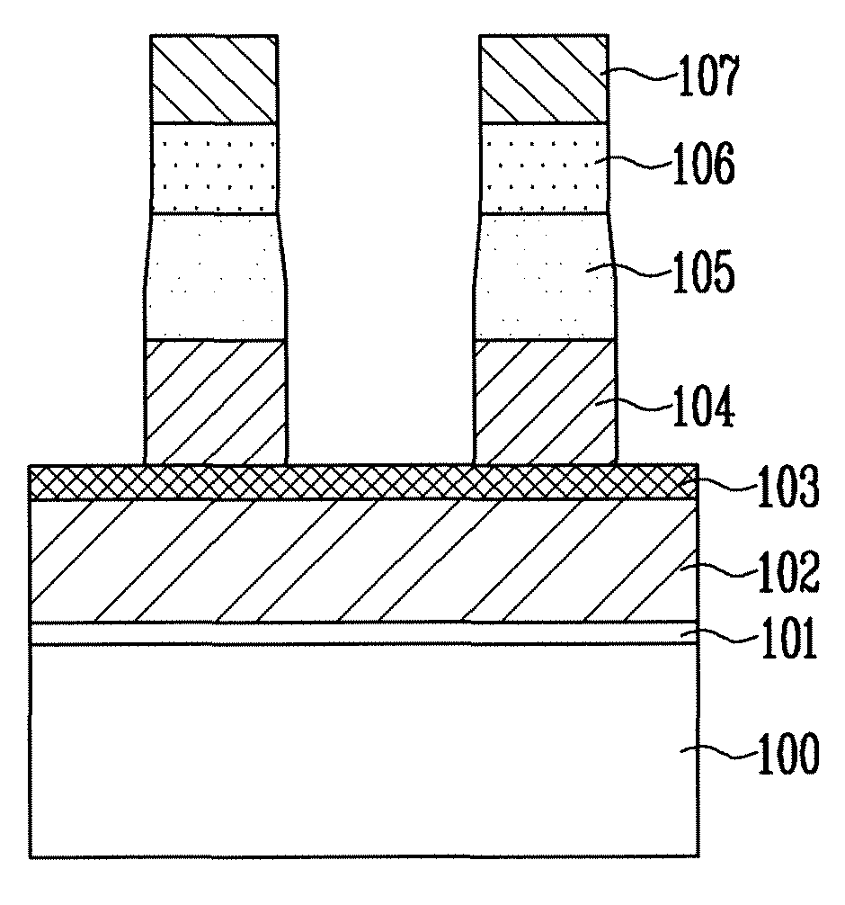
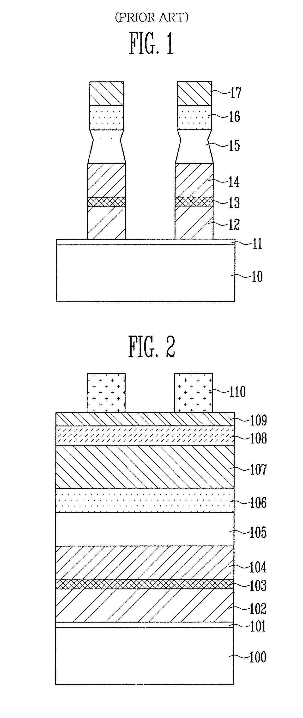
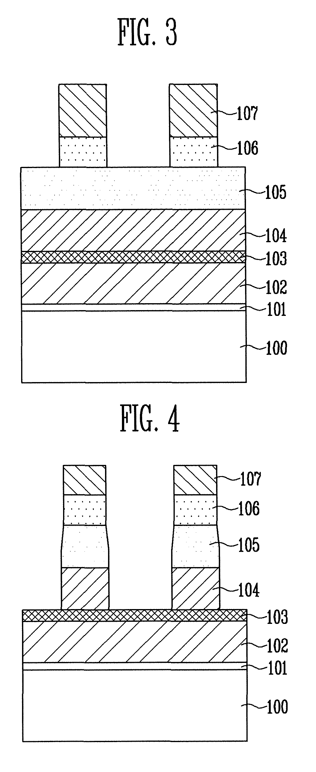
[0016]Referring to FIG. 2, a tunnel dielectric layer 101 may be formed on a semiconductor substrate 100. The tunnel dielectric layer 101 may be formed, for example, from an oxide film. A conductive layer 102 for a floating gate may be formed over the entire surface, including the tunnel dielectric layer 101. The conductive layer 102 for the floating gate may be formed, for example, from a polysilicon film. A dielectric layer 103, a conductive layer 104 for a control gate, and a metal electrode layer 105 may be formed over the entire surface, including the conductive layer 102 for the floating gate. The dielectric layer 103, the conductive layer 104 for a control gate, and the metal electrode layer 105 may be formed sequentially over the entire surface. The dielectric layer 10...
PUM
| Property | Measurement | Unit |
|---|---|---|
| conductive | aaaaa | aaaaa |
| dielectric | aaaaa | aaaaa |
| pressure | aaaaa | aaaaa |
Abstract
Description
Claims
Application Information
 - R&D
- Intellectual Property
- Life Sciences
- Materials
- Tech Scout
- Unparalleled Data Quality
- Higher Quality Content
- 60% Fewer Hallucinations
Browse by: Latest US Patents, China's latest patents, Technical Efficacy Thesaurus, Application Domain, Technology Topic, Popular Technical Reports.
© 2025 PatSnap. All rights reserved.Legal|Privacy policy|Modern Slavery Act Transparency Statement|Sitemap|About US| Contact US: help@patsnap.com