Nonvolatile latch circuit and nonvolatile flip-flop circuit
a latch circuit and non-volatile technology, applied in the direction of pulse technique, digital storage, instruments, etc., can solve the problems of fine circuit fine reduction of readout margin, restricted block to which the technique can be applied, etc., and achieve excellent scalability and high endurance
- Summary
- Abstract
- Description
- Claims
- Application Information
AI Technical Summary
Benefits of technology
Problems solved by technology
Method used
Image

Examples
first embodiment
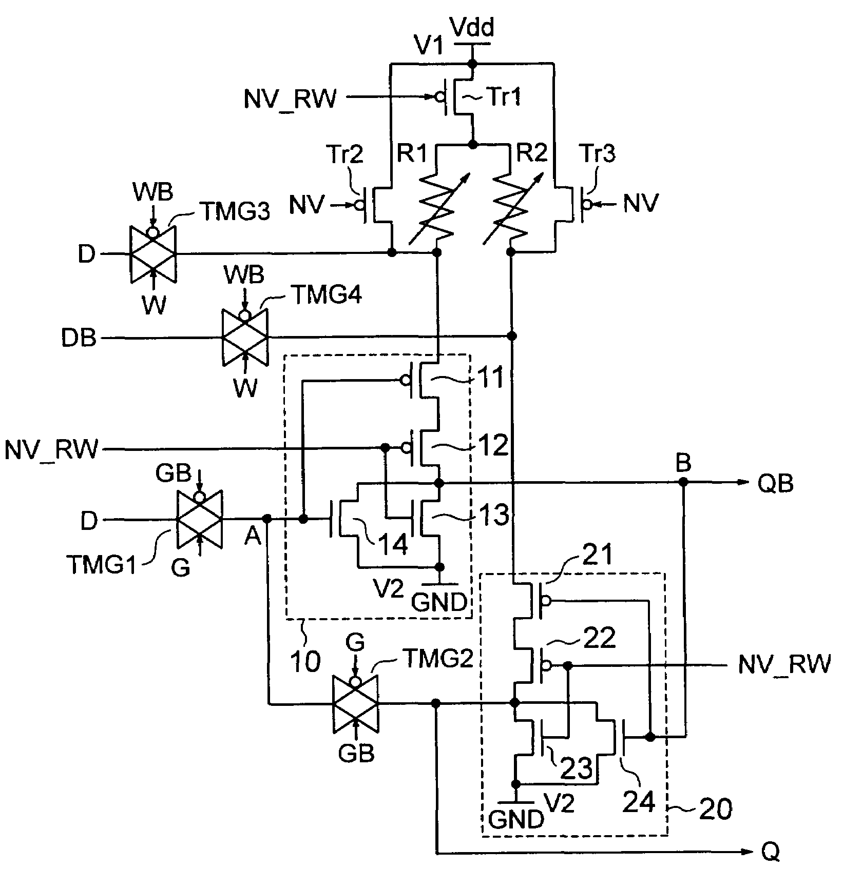
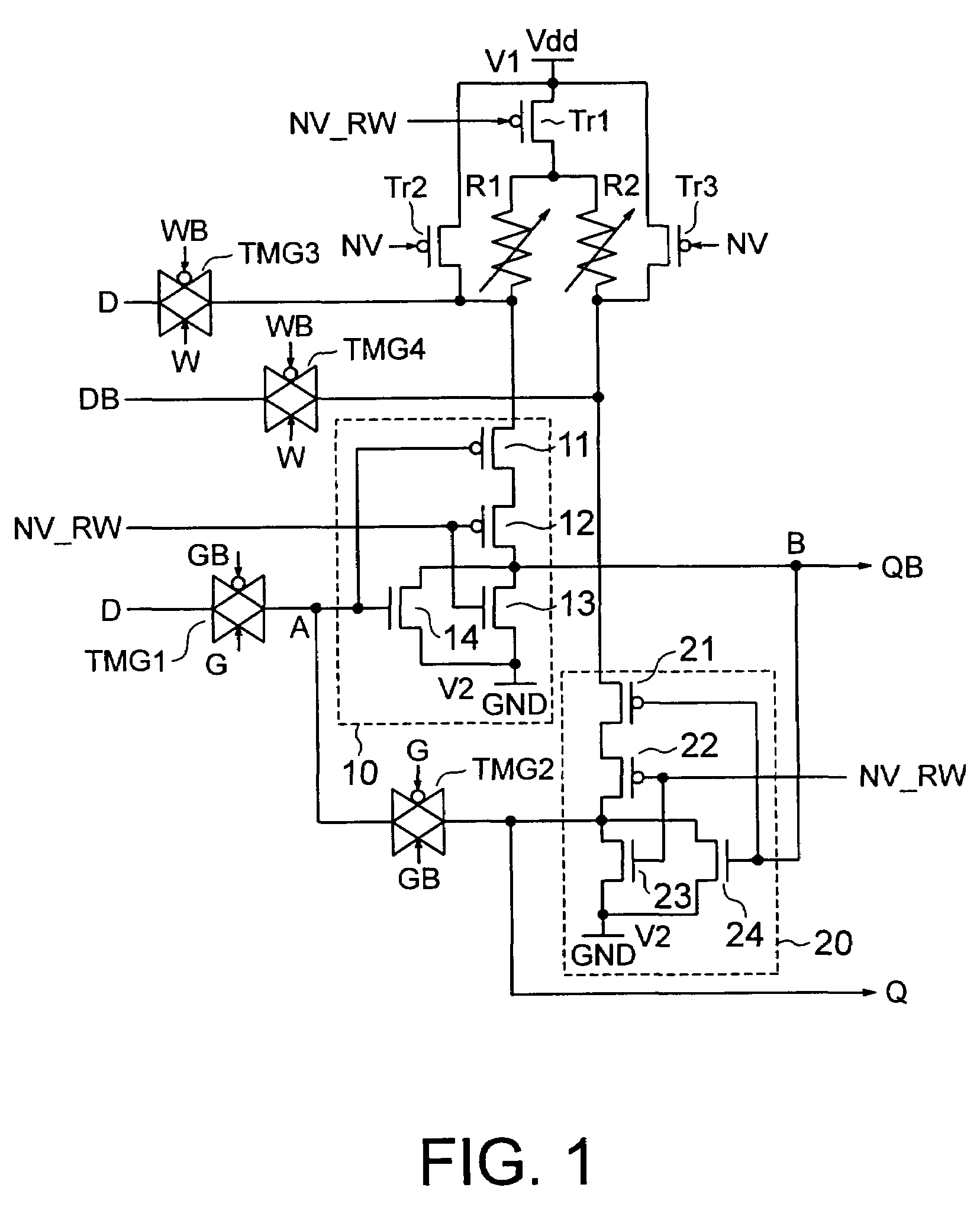
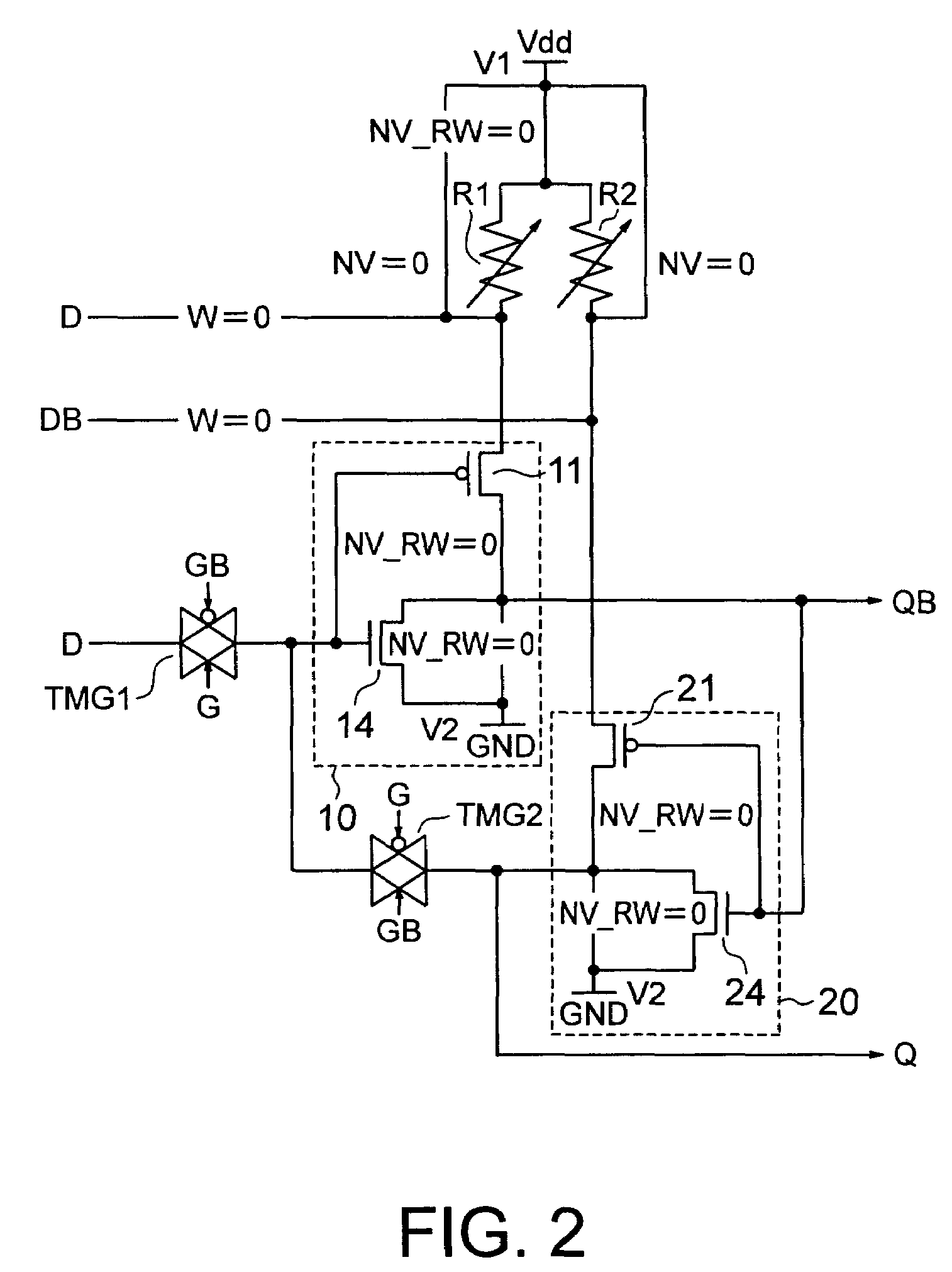
[0037]A nonvolatile latch circuit according to a first embodiment of the present invention is shown in FIG. 1. The nonvolatile latch circuit according to the present embodiment includes logic circuits 10 and 20, spin injection type MTJ (Magnetic Tunnel Junction) elements R1 and R2, p-channel transistors Tr1, Tr2 and Tr3, and transmission gates TMG1, TMG2, TMG3 and TMG4.
[0038]The logic circuits 10 and 20 are configured so as to output a definite logic value (“0” in the present embodiment) or operate as an inverter according to a control signal NV_RW.
[0039]In a specific example of the logic circuit 10, a series circuit composed of p-channel transistors 11 and 12 connected in series and a parallel circuit composed of n-channel transistors 13 and 14 connected in parallel are connected in series. Gates of the p-channel transistor 12 and the n-channel transistor 13 are connected in common to receive the control signal NV_RW. Gates of the p-channel transistor 11 and the n-channel transisto...
second embodiment
[0058]A nonvolatile latch circuit according to a second embodiment of the present invention is shown in FIG. 6(a). The nonvolatile latch circuit according to the present embodiment includes logic circuits 30 and 40, spin injection type MTJ (Magnetic Tunnel Junction) elements R1 and R2, n-channel transistors Tr4, Tr5 and Tr6, and transmission gates TMG1, TMG2, TMG3 and TMG4.
[0059]The logic circuits 30 and 40 are configured so as to output a definite logic value (“1” in the present embodiment) or operate as an inverter according to a control signal NV_RWB.
[0060]In a specific example of the logic circuit 30, a parallel circuit composed of p-channel transistors 31 and 32 connected in parallel and a series circuit composed of n-channel transistors 33 and 34 connected in series are connected in series. Gates of the p-channel transistor 32 and the n-channel transistor 33 are connected in common to receive the control signal NV_RWB. Gates of the p-channel transistor 31 and the n-channel tra...
third embodiment
[0076]A nonvolatile latch circuit according to a third embodiment of the present invention is shown in FIG. 7. The nonvolatile latch circuit according to the present embodiment has a configuration obtained from the nonvolatile latch circuit according to the first embodiment shown in FIG. 1 by disposing a transmission gate TMG5 having the same size as that of the transmission gate TMG2 between the output of the logic circuit 10 and the input of the logic circuit 20 in order to attain impedance matching between nodes located on the left and right sides of the cross-coupled logic circuits 10 and 20.
[0077]Owing to such a configuration, it becomes easy to read out a difference in resistance value between the spin injection type MTJ elements R1 and R2. GND or Vdd is connected to gates of the transmission gate TMG5 so as to always bring the transmission gate TMG5 into the ON state.
[0078]In the present embodiment as well, the nonvolatile latch circuit which is excellent in scalability even ...
PUM
 Abstract
Description
Claims
Application Information
 - R&D
- Intellectual Property
- Life Sciences
- Materials
- Tech Scout
- Unparalleled Data Quality
- Higher Quality Content
- 60% Fewer Hallucinations
Browse by: Latest US Patents, China's latest patents, Technical Efficacy Thesaurus, Application Domain, Technology Topic, Popular Technical Reports.
© 2025 PatSnap. All rights reserved.Legal|Privacy policy|Modern Slavery Act Transparency Statement|Sitemap|About US| Contact US: help@patsnap.com