Method for fabricating thin film pattern, method for fabricating device, electro-optical apparatus, and electronic apparatus

a thin film pattern and fabrication method technology, applied in the direction of non-linear optics, identification means, instruments, etc., can solve the problems of generating puddles (bulges) of liquid, high production costs, and most materials, and achieves the effect of reducing the liquid-repellency of the surface at this part, easy adjustment, and reducing the thickness of the film

Inactive Publication Date: 2010-05-11
SEIKO EPSON CORP
View PDF29 Cites 7 Cited by
  • Summary
  • Abstract
  • Description
  • Claims
  • Application Information

AI Technical Summary

Benefits of technology

[0011]According to the present invention, since the first liquid droplets made of a function liquid are disposed on the substrate at the first material disposing step, an intermediate drying treatment is performed on the function liquid on the substrate to dry the function liquid (film pattern), and then, the second liquid droplets made of the next function liquid are disposed on this dried function liquid at the second material disposing step, the second liquid droplets are disposed smoothly on the film of the function liquid formed by the intermediate drying treatment on the substrate. By repeatedly performing this treatment several times, a thick film pattern can be formed smoothly with a predetermined thickness. In addition, since the function liquid are disposed between the banks standing on the substrate in order to form the film pattern, the film pattern with a predetermined shape can be smoothly patterned along the shapes of the banks.
[0026]According to the present invention, a thick film pattern can be formed smoothly with a predetermined thickness. In addition, since the function liquid are disposed between the banks standing on the substrate in order to form the film pattern, the film pattern with a predetermined shape can be smoothly patterned along the shapes of the banks. Therefore, an active matrix substrate with a predetermined performance can be manufactured.

Problems solved by technology

In this photolithography process, large facilities such as vacuum equipment and complicated processes are necessary, efficiencies in the use of materials are around a few percent, that is, most of the materials is discarded, and production costs are high.
In the case of forming a thick film pattern using a liquid droplet ejecting process, a method in which a larger-size droplet is ejected can be conceived, but this method has disadvantages such as generation of puddles (bulges) of liquid.

Method used


Image

  • Method for fabricating thin film pattern, method for fabricating device, electro-optical apparatus, and electronic apparatus
  • Method for fabricating thin film pattern, method for fabricating device, electro-optical apparatus, and electronic apparatus
  • Method for fabricating thin film pattern, method for fabricating device, electro-optical apparatus, and electronic apparatus

Examples


Embodiment Construction

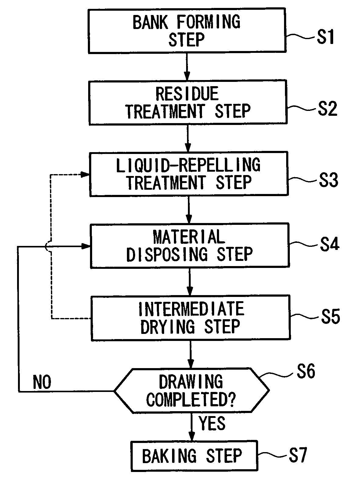
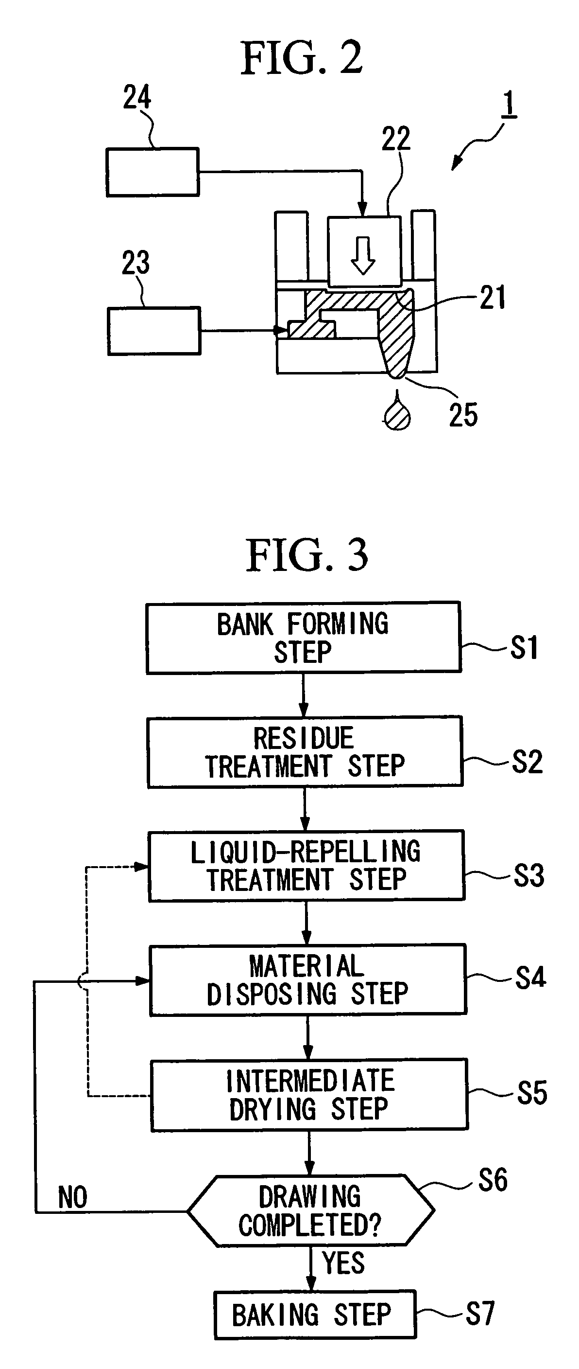
[0047]An embodiment of a method for fabricating a thin film pattern on a substrate and a method for manufacturing a device, according to the present invention, will be explained with reference to the figures. As an example of this embodiment, a case in which an ink (function liquid) for forming patterns of lines (patterns of thin films), in which conductive fine particles are included, is ejected on a substrate in the form of liquid droplets from nozzles of an ejecting head using a liquid droplet ejecting process, and line patterns formed of conductive films on the substrate, will be explained.

[0048]First, an ink (function liquid) which is used is explained. The ink for line patterns of a liquid material, is made of a dispersion liquid, which includes a dispersion medium and conductive fine particles that are dispersed in the dispersion medium, or a solution in which organosilver compound or silver oxide nanometer particles are dispersed (or dissolved) in a solvent (dispersion mediu...


PUM

PropertyMeasurementUnit
sizesaaaaaaaaaa
sizesaaaaaaaaaa
surface tensionaaaaaaaaaa

Abstract

A method for fabricating a thin film pattern on a substrate includes a bank forming step of forming banks in a predetermined pattern on said substrate, a first material disposing step of disposing first liquid droplets made of a function liquid between said banks to form a first pattern, a second material disposing step of disposing second liquid droplets made of a function liquid on said first pattern, and an intermediate drying step of removing at least a part of a solvent contained in said first liquid droplets between said first material disposing step and said second material disposing step.

Description

BACKGROUND OF THE INVENTION[0001]1. Field of the Invention[0002]The present invention relates to a method for fabricating a thin film pattern, a method for manufacturing a device, an electro-optical apparatus, and an electronic apparatus.[0003]Priority is claimed on Japanese Patent Application No. 2003-155861, filed May 30, 2003, and Japanese Patent Application No. 2004-94527, filed Mar. 29, 2004, the contents of which are incorporated herein by reference.[0004]2. Description of Related Art[0005]A photolithography process is used in manufacturing a device with lines (wiring) such as electronic circuits and integrated circuits. In this photolithography process, line patterns of thin films are formed by applying a photosensitive material, a so-called resist, on a conductive film preliminarily applied on a substrate, irradiating the resist in a circuit pattern and developing, and etching the conductive film in the resist pattern. In this photolithography process, large facilities such ...

Claims


Application Information

Patent Timeline
Patent Type & Authority Patents(United States)
IPC IPC(8): G03F9/00G02F1/1343G02F1/1345G02F1/1362G02F1/1368G09F9/00G09F9/30H01L21/208H01L21/28H01L21/288H01L21/3205H01L21/336H01L21/77H01L21/84H01L27/12H01L27/32H01L29/786H01L51/00H01L51/40H01L51/50H01L51/56H05B33/10H05B33/12H05K3/12
CPCH01L21/288H01L27/12H01L27/14687H01L27/1292H01L51/0021G02F2001/136295H01L27/3295H01L51/0005H05K3/1241H01L27/3244G02F1/136295H10K71/135H10K59/122H10K71/60H10K59/12H01L27/1214
Inventor HIRAI, TOSHIMITSU
Owner SEIKO EPSON CORP
Why Eureka
Try Eureka