Eureka AIR delivers breakthrough ideas for toughest innovation challenges, trusted by R&D personnel around the world.

Solid-state image pickup device

a solid-state image and pickup device technology, applied in the direction of radio frequency control devices, television system scanning details, television systems, etc., can solve the problems of low sensitivity, color mixing, wiring layout, etc., and achieve the effect of low cost and controllable sensitivity and color mixing

Inactive Publication Date: 2010-04-20
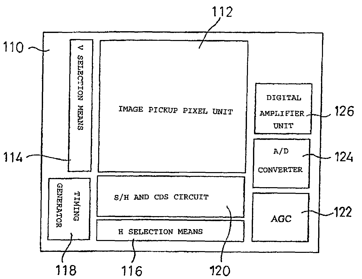
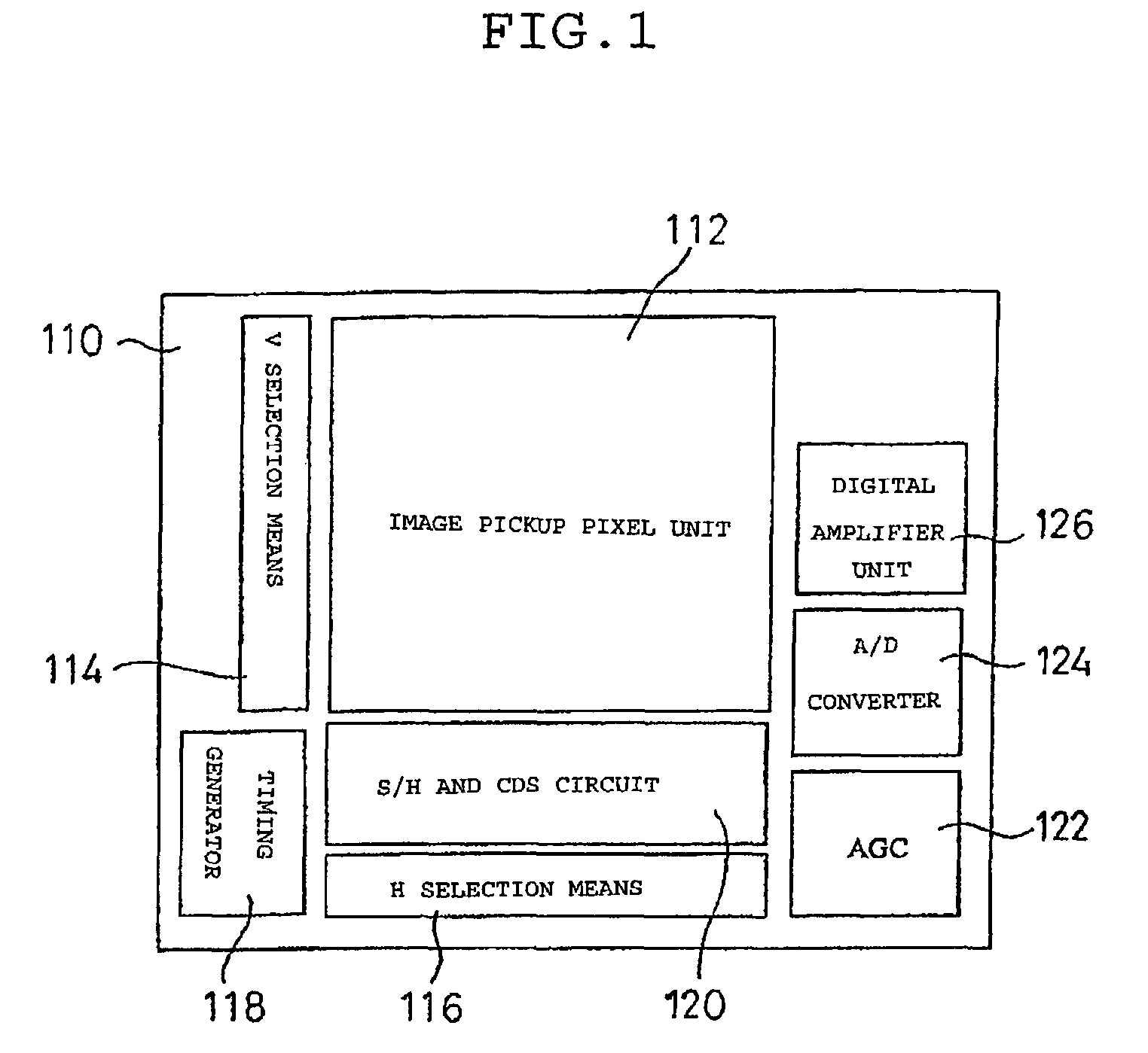
SONY SEMICON SOLUTIONS CORP
View PDF9 Cites 61 Cited by
  • Summary
  • Abstract
  • Description
  • Claims
  • Application Information

AI Technical Summary

Benefits of technology

[0045]With the solid-state image pickup device and the method of fabricating the same according to the present invention, the electric field generating means is provided which generates an electric field in the semiconductor substrate in the direction of depth of the semiconductor substrate and thereby leads photoelectrons entering from the second surface (light receiving plane) of the semiconductor substrate to the photoelectric converting device formed on the first surface side of the semiconductor substrate. Therefore, even when the photoelectric converting device and a well region are formed in a shallow region on the first surface side of the semiconductor substrate, photons entering from the second surface of the semiconductor substrate can be effectively led to the photoelectric converting device. It is thereby possible to control decrease in sensitivity and color mixing.

Problems solved by technology

1) The reflection by the wiring of the part of the light condensed by the microlens 19 correspondingly lowers sensitivity.
2) A part of the light reflected by the wiring enters a photodiode of an adjacent pixel, resulting in color mixing.
3) Since wiring layout is limited, limitations in that wiring cannot be placed over the photodiode or thick wiring cannot be routed degrade characteristics.
4) Size reduction is difficult for the same reason as in 3).
5) Light obliquely enters a pixel in a peripheral portion and is therefore reflected at a higher rate, resulting in darker shading in the peripheral portion.
6) When the CMOS image sensor is to be produced by an advanced CMOS process involving more wiring layers, a distance from the microlens to the photodiode is increased, which aggravates the difficulties as described above.
7) As a result of 6), a library of the advanced CMOS processes cannot be utilized. Laying out again of circuits registered in the library, increase in area due to limitations on the wiring layers or the like results in increased cost. Also, pixel area per pixel is increased.
When the electrons enter a pixel shielded from light for black detection, a black level is erroneously detected.
This increases and complicates process steps.
A defect in the photodiode is also caused by the process steps.
Thus, with the conventional method of passing light through wiring layers to the light receiving plane, light cannot be condensed on the light receiving plane of the pixel efficiently, and the problems of 1) to 7) are more noticeable.
However, the forming of the P-type well regions to a depth of 10 ,,m or more in the semiconductor substrate has a problem in that it requires advanced fabrication technology.
This causes problems of color mixing and decrease in resolution.

Method used


Image

  • Solid-state image pickup device
  • Solid-state image pickup device
  • Solid-state image pickup device

Examples


Embodiment Construction

[0059]A preferred embodiment of a solid-state image pickup device and a method of fabricating the same according to the present invention will hereinafter be described.

[0060]The solid-state image pickup device according to the present embodiment is a rear surface incidence type CMOS image sensor having a wiring layer on a first surface of a semiconductor substrate (device forming layer) where a photodiode, a reading circuit and the like are disposed, and a light receiving plane in a second surface. In the rear surface incidence type CMOS image sensor, the photodiode and a P-type well region on the periphery of the photodiode are disposed in a layer structure that does not reach the rear surface (light receiving surface) of the substrate, and an electric field is formed within the substrate to properly lead electrons entering from the rear surface (light receiving surface) of the substrate to the photodiode.

[0061]That is, even with the layer structure with a distance between the ligh...


PUM


Abstract

In a rear surface incidence type CMOS image sensor having a wiring layer 720 on a first surface (front surface) of an epitaxial substrate 710 in which a photodiode, a reading circuit (an n-type region 750 and an n+ type region 760) and the like are disposed, and a light receiving plane in a second surface (rear surface), the photodiode and a P-type well region 740 on the periphery of the photodiode are disposed in a layer structure that does not reach the rear surface (light receiving surface) of the substrate, and an electric field is formed within the substrate 710 to properly lead electrons entering from the rear surface (light receiving surface) of the substrate to the photodiode. The electric field is realized by providing a concentration gradient in a direction of depth of the epitaxial substrate 710. Alternatively, the electric field can be realized by providing a rear-surface electrode 810 or 840 for sending a current.

Description

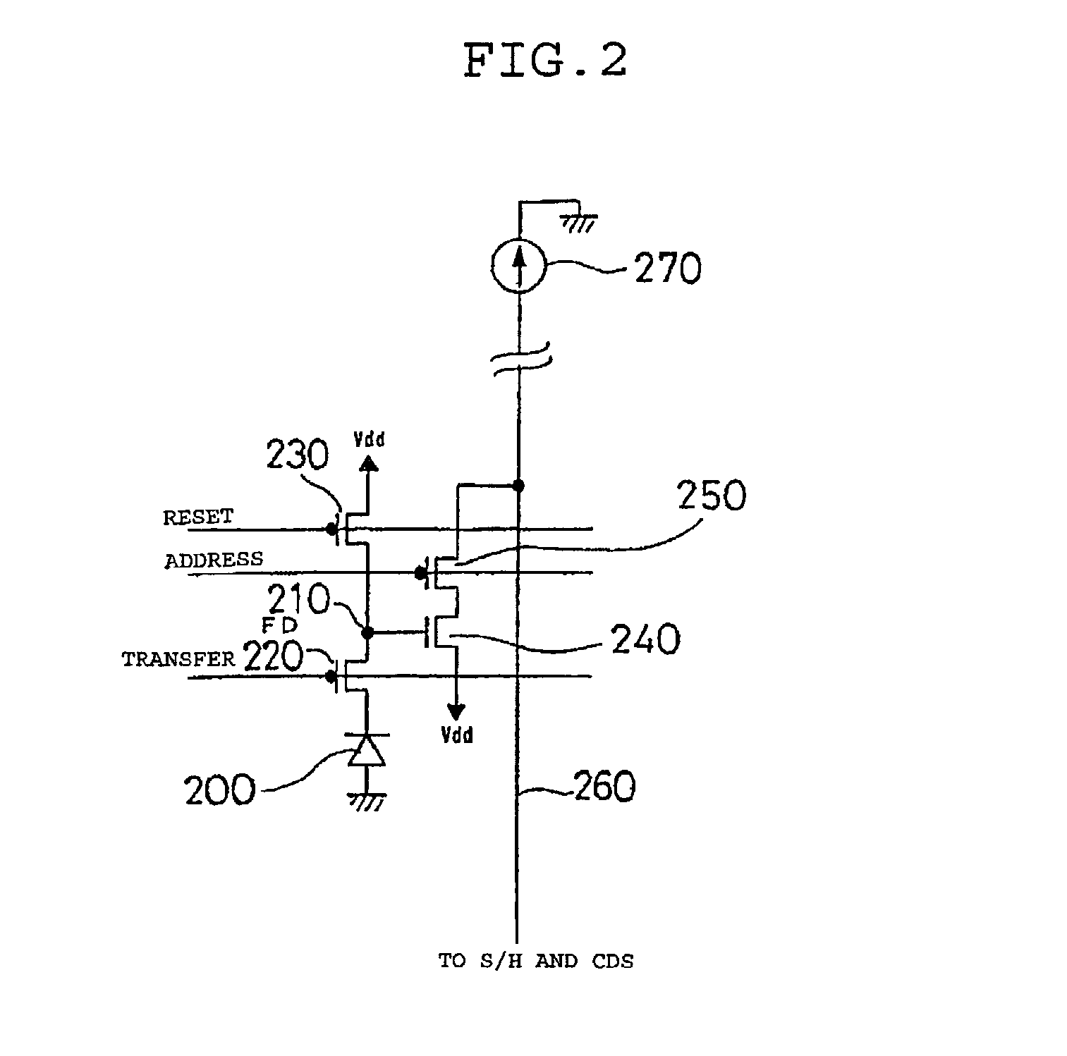
[0001]This application claims priority to previously filed Japanese patent application number P2002-144886 filed on May 20, 2002, in JAPAN which is incorporated herein by reference.BACKGROUND OF THE INVENTION[0002]The present invention relates generally to a solid-state image pickup device for use as various image sensors and camera modules.DESCRIPTION OF THE RELATED ART[0003]Recently, video cameras and electronic cameras have achieved tremendous commercial success. These cameras typically use a CCD type or an amplification type solid-state image pickup device.[0004]Of the conventional solid-state image pickup devices, the amplification type solid-state image pickup device (CMOS image sensor) includes, on a single semiconductor chip, an image pickup pixel unit formed by arranging a plurality of pixels two-dimensionally and a peripheral circuit unit disposed on the outside of the image pickup pixel unit.[0005]Each of the pixels of the image pickup pixel unit includes an FD part and v...

Claims


Application Information

Patent Timeline
IPC IPC(8): H01L31/113H01L27/14H01L27/146
CPCH01L27/14618H01L27/14621H01L27/14627H01L27/14643H01L27/1464H01L27/14689H01L2924/3025H01L2224/48091H01L2924/01046H01L2924/13091H01L2924/00014H01L2924/00
Inventor MABUCHI, KEIJI
Owner SONY SEMICON SOLUTIONS CORP
Why Eureka
Eureka Blog
Learn More