
Sensing device

a technology of sensing device and amplitude signal, which is applied in the direction of vibration measurement in solids, analysis of fluids using sonic/ultrasonic/infrasonic waves, instruments, etc. it can solve the problems of inconvenient use, unstable frequency, and considerable amplitude level of frequency signal when using in liquids, so as to achieve stable oscillation, reduce size, and high negative resistance

Inactive Publication Date: 2010-04-06
NIHON DEMPA KOGYO CO LTD
View PDF6 Cites 4 Cited by
  • Summary
  • Abstract
  • Description
  • Claims
  • Application Information

AI Technical Summary

Benefits of technology

[0026]An object of the present invention is to provide a sensing device which can exhibit high negative resistance required to the sensing device, realize down sizing of the sensing device and reduction of manufacturing costs by making the amplitude control circuit unnecessary, and further realize stable oscillation toward temperature variations.
[0037]As described above, according to the present invention, by optimizing the constant of the Colpitts oscillation circuit formed with a quartz resonator and a transistor amplifier circuit, it is possible to obtain the stable oscillation by securing a high negative resistance required by the sensing device, and achieve reduction in size and reduction in manufacturing costs of the sensing device by making the amplitude control circuit unnecessary. Furthermore, it can realize stable oscillation toward temperature variations.

Problems solved by technology

In such a case, when set as a circuit to oscillate a quartz resonator in a liquid, some inconvenience occurs when measuring, for instance, components in the air.
That is, the amplitude of quartz resonator oscillation becomes great, resulting in secondary oscillation due to extreme smallness of viscosity of gases compared with that of liquids, and therefore the frequency becomes unstable.
Conversely, when set as a circuit to oscillate the quartz resonator in the air, the amplitude level of the frequency signal when using in a liquid is considerably high compared with that in the air, and therefore, accurate frequency measurement can not be conducted in a signal processing unit at the following step.
This kind of problem would happen even in the case of using the device in a liquid.
Thus, when the viscosity in a measuring medium (liquid) to conduct measurement of a sensing target differs, the amplitude of the frequency signal also differs, which causes a problem of limiting the scope of application of the measuring medium.
For instance, it is difficult to build up a sensing device applicable for both gas and liquid.
Furthermore, when the frequency signal from an oscillation circuit is digitally processed to measure the frequency, if the amplitude level of the frequency signal is out from a limited narrow range, the error in measurement can become great.
Accordingly, when conducting a digital processing, it is difficult to widen the scope of application of the measuring medium especially, which brings another disadvantage.

Method used


Image

  • Sensing device
  • Sensing device
  • Sensing device

Examples


embodiment 1

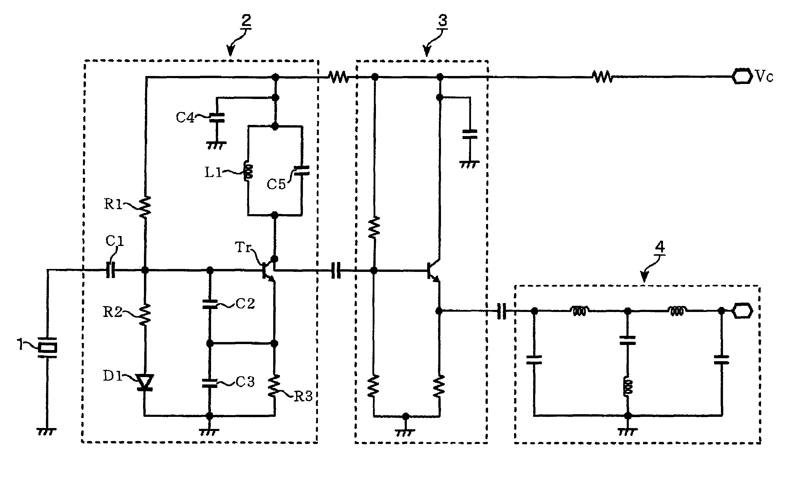
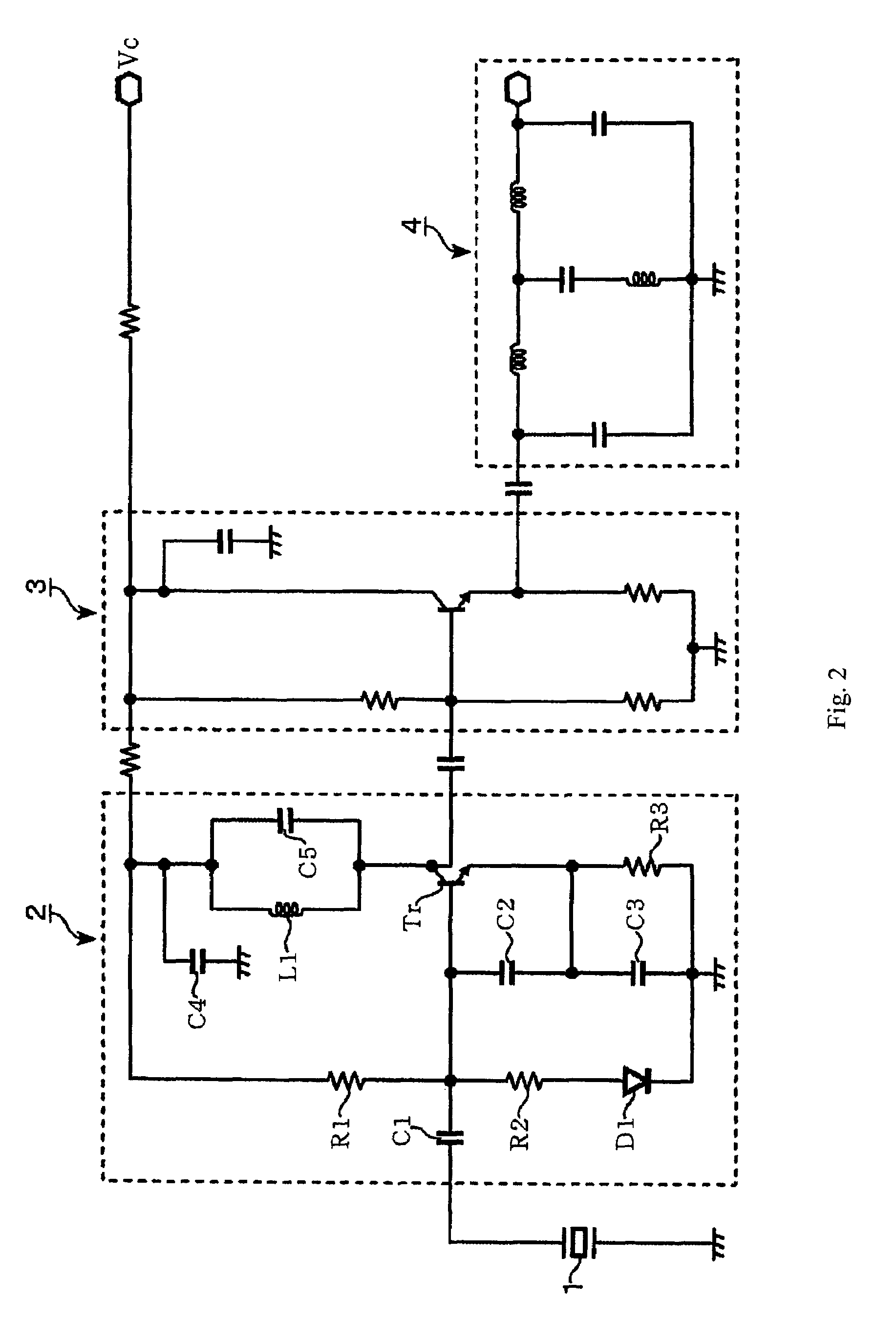
[0051]FIG. 1 is a block diagram of a sensing device showing an embodiment of the present invention. The difference from FIG. 11 is the structure omitting an amplitude control circuit 6 and a second buffer amplifier 5. FIG. 2 is a circuit diagram showing the structures of respective blocks in FIG. 1 in detail.

[0052]Firstly, in the present embodiment, the sensing device having an oscillation frequency of 30.8 MHz is assumed. In this oscillation frequency, the impedance of a tuning circuit connected to the output unit of an oscillation amplifier element of a Colpitts oscillation circuit 2 is set at a value having inductivity in the oscillation frequency. In more specific, a tuning circuit 20 composed of a parallel circuit of an inductor L1 and a capacitor C5 is provided between a collector of a transistor Tr (BJT-NPN) and a supply source Vc. The inductor L1 and the capacitor C5 are set at 4.7 uH and 3 pF respectively, so that they are composed as a tuning circuit exhibiting inductivity...

embodiment 2

[0055]Although the peak of the negative resistance in FIG. 3 is about 400 Ω, a method of increasing the negative resistance will be explained hereinafter giving an example. In the present embodiment, by limiting the capacity ratio of a pair of capacitors C2 and C3 for capacity division, and the impedance at the oscillation frequency in a Colpitts oscillation circuit in which the tuning circuit 20 in Embodiment 1 is made inductive, improvement of the negative resistance is attempted. In specific, the respective capacity of the capacitor C2 connected between a base and an emitter of the transistor Tr as an amplifying element for oscillation, and the capacitor C3 connected between the emitter and a ground (GND) are determined as follows. The ratio of the impedance at the oscillation frequency of the capacitor C2 to the impedance at the oscillation frequency, for instance, 30.8 MHz of the capacitor C3 is set at 3 or more. In other words, the ratio of the capacity of the capacitor C2 to ...

embodiment 3

[0063]In the present embodiment, by making the tuning circuit inductive as in Embodiment 1, and by setting the bias resistance connected between the collector and the base of an amplifying element for oscillation to be 3 kΩ or less in a Colpitts oscillation circuit in which the capacitance ratio of the capacitors C2 and C3 and the impedance of the capacitor C2 are limited as in Embodiment 2, reduction of the negative resistance is prevented. For instance, the bias resistance R1 in FIG. 2 is set to 1.2 kΩ.

[0064]FIG. 9 shows a negative resistance characteristic when the bias resistance R1 is varied. As the test conditions at this time, the capacitor C2 has an impedance of 300 Ω at the oscillation frequency, and C2 / C3=⅓.

[0065]In the figure, the characteristic A is the case of R1=2 kΩ, the characteristic B is R1=3 kΩ, and the characteristic C is R1=4 kΩ. In order to obtain a negative characteristic of 1 kΩ or more at the oscillation frequency from the characteristic, the characteristic ...


PUM

PropertyMeasurementUnit
impedanceaaaaaaaaaa
bias resistanceaaaaaaaaaa
oscillation frequencyaaaaaaaaaa

Abstract

To provide a Colpitts oscillation circuit formed with a quartz resonator and a transistor amplifier circuit, which can secure sufficient negative resistance, obtain stable oscillation, negate the need for an amplitude control circuit, and realize stabilization against temperature variations. In order to solve the problem, a structure in which the impedance of a tuning circuit provided in a collector of the transistor exhibits inductivity at the oscillation frequency is provided. The impedance ratio at the oscillation frequency of a capacitor C2 connected between a base and an emitter to a capacitor C3 connected between the emitter and a ground, of the transistor is set at 3 to 1 or more. Furthermore, the impedance of capacity C2 connected between the base and the emitter at the oscillation frequency is set at 300 Ω or more. A bias resistance R1 connected between the collector and the base of the transistor is set at 3 kΩ or less. A temperature compensation diode D1 is inserted in series between the base and the ground (GND) between the transistor.

Description

BACKGROUND OF THE INVENTION[0001]1. Field of the Invention[0002]The present invention relates to a sensing device which is provided with an adsorption layer for adsorbing a sensing target on an electrode surface of a piezoelectric resonator such as a quartz resonator, and detects and measures the sensing target based on variation in natural frequency of the quartz resonator caused by adsorption of the sensing target to the adsorption layer, especially to a Colpitts oscillation circuit formed with a quartz resonator and a transistor amplifier circuit.[0003]2. Description of the Related Art[0004]This kind of the sensing devices is commercially practical as a device which, for instance, combines a substance to be measured with the antibody to make an immune reaction with the substance to be measured, utilizing an antigen-antibody reaction as an immune reaction, and detects and measures the substance to be measured based on the degree of the reaction.[0005]FIG. 10 shows a basic structur...

Claims


Application Information

Patent Timeline
Patent Type & Authority Patents(United States)
IPC IPC(8): H03B5/38G01H13/00G01H3/08G01N29/036
CPCH03B5/362H03L5/00H03L1/02
Inventor ISHII, TAKEHITOWAKAMATSU, SHUNICHI
Owner NIHON DEMPA KOGYO CO LTD
Learn More