
an oscillating circuit

A technology of oscillating circuit and oscillating module, applied in the direction of heating element shape, etc., can solve the problems of difficulty in meeting the requirements of small circuit size, large capacitance occupying wafer area, high circuit cost, etc., to achieve good performance and ensure oscillation amplitude , The effect of reducing the wafer area

Active Publication Date: 2022-06-17
深圳昂瑞微电子技术有限公司
View PDF0 Cites 0 Cited by
  • Summary
  • Abstract
  • Description
  • Claims
  • Application Information

AI Technical Summary

Problems solved by technology

[0004] In the crystal oscillator circuit in the prior art, in order to increase the negative resistance of the circuit under the condition of limited current, it is necessary to set a relatively large MOM capacitor to make the transconductance negative resistance of the pull-up transistor work, and the large capacitor occupies a large amount of energy. The wafer area is not only difficult to meet the requirements of small circuit size, but also the larger wafer area makes the circuit cost high

Method used


Image

  • an oscillating circuit
  • an oscillating circuit
  • an oscillating circuit

Examples


Embodiment Construction

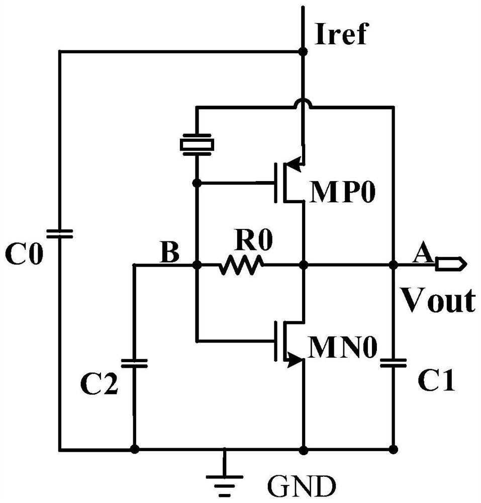
[0047] As described in the background art, in order to improve the negative resistance of the circuit under the condition of limited current in the crystal oscillator circuit in the prior art, a relatively large MOM capacitor needs to be set to make the transconductance negative resistance of the pull-up transistor work. Specifically, refer tofigure 1 , figure 1 It is a schematic diagram of the circuit structure of a traditional oscillator circuit. The first transistor MP0, the second transistor MN0, the first resistor R0, the first capacitor C0, the second capacitor C1 and the third capacitor C2 are formed. For the specific connection relationship, refer to figure 1 , the first transistor MP0 is a P-type transistor, and the second transistor MN0 is an N-type transistor. figure 1 Among them, A and B represent the internal nodes of the circuit, GND represents the ground, Vout represents the output terminal, and Iref represents the reference current provided by the system.

[0...


PUM


Abstract

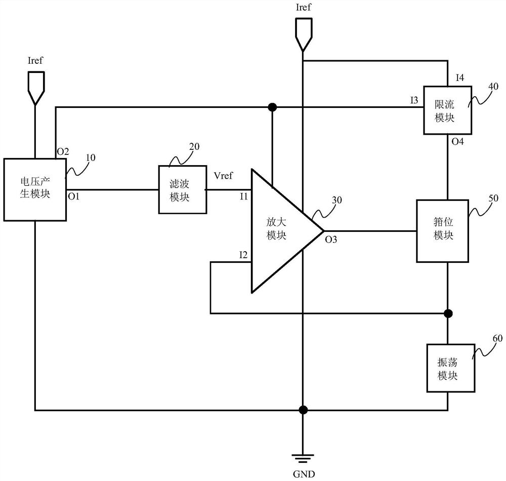
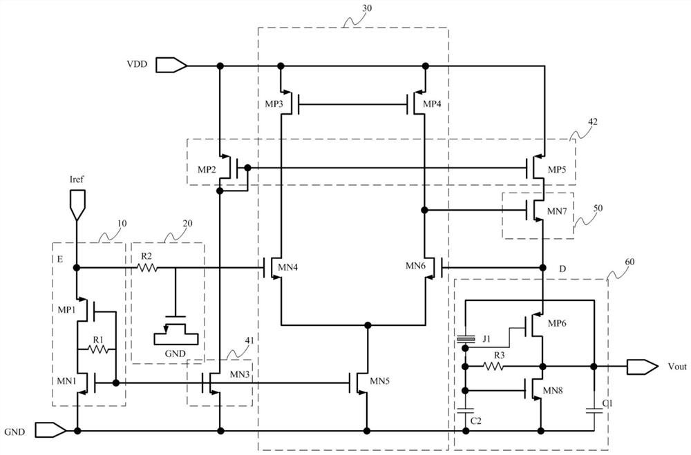
The present application discloses an oscillating circuit. The amplifying module and the clamping module of the oscillating circuit constitute a low-dropout linear voltage regulator, which limits the potential of the second terminal of the clamping module to a preset voltage. Since the second terminal of the clamping module The output impedance of the terminal is very small within the bandwidth of the amplifying module, which can provide this point with the effect similar to the AC virtual ground. The virtual ground effect of this point makes the oscillation module realize the improvement at low frequencies without a large capacitor occupying a large wafer area. The purpose of the negative resistance of the circuit is beneficial to reduce the wafer area required by the oscillator circuit. In addition, due to the existence of the low-dropout linear voltage regulator, even if the capacitance in the oscillation module is adjusted to meet the consistency of the wafer, it will not cause the potential change of the second terminal of the clamp module, and the final output oscillation signal The upper limit will not change, which is beneficial to ensure the oscillation amplitude of the oscillation signal output by the oscillation circuit and ensure that the oscillation circuit has good performance.

Description

technical field [0001] The present application relates to the technical field of integrated circuits, and more particularly, to an oscillator circuit. Background technique [0002] Crystal oscillators have found numerous applications in various electronic systems. With the continuous development of wireless communication technology and the popularization of portable mobile devices, the clock signal has become a necessary signal for the cooperative work of various internal devices. [0003] Real Time Clock (RTC) signals are used in many digital integrated circuits. The key part of generating real time clock signals is the 32.768kHz crystal oscillator circuit. The circuit has put forward newer and higher requirements, which are concentrated in the aspects of high stability, wide power supply voltage range, small area, low power consumption and low cost. [0004] In order to improve the negative resistance of the circuit under the condition of limited current in the crystal o...

Claims


Application Information

Patent Timeline
Patent Type & Authority Patents(China)
IPC IPC(8): H05B3/50
CPCH05B3/50
Inventor 闫广钱永学周晓秋孟震一刘澎孙晓菲蔡光杰孟浩黄鑫
Owner 深圳昂瑞微电子技术有限公司
Learn More