a chip
A chip and pin technology, applied in the field of chips, can solve the problems of waste and limitation of chip area, and achieve the effect of reducing wafer area and cost
- Summary
- Abstract
- Description
- Claims
- Application Information
AI Technical Summary
Problems solved by technology
Method used
Image
Examples
Embodiment 1
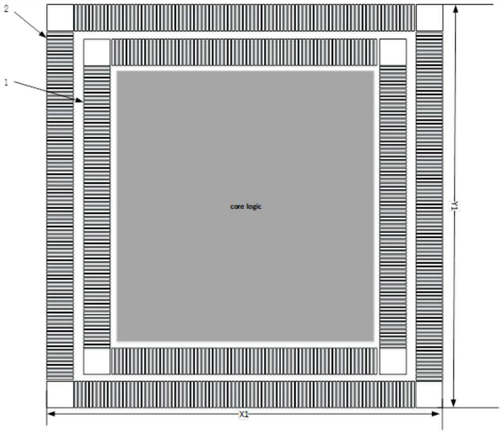
[0025] Refer to the attached figure 2 and attached Image 6 , the invention discloses a chip, which includes core logic and input and output pins, and input and output pins are arranged around the core logic; the input and output pins include: a first circle of input and output pins and a second circle of input and output pins Output pins; the core logic is arranged in the first circle of input and output pins, and the first circle of input and output pins is arranged in the second circle of input and output pins.
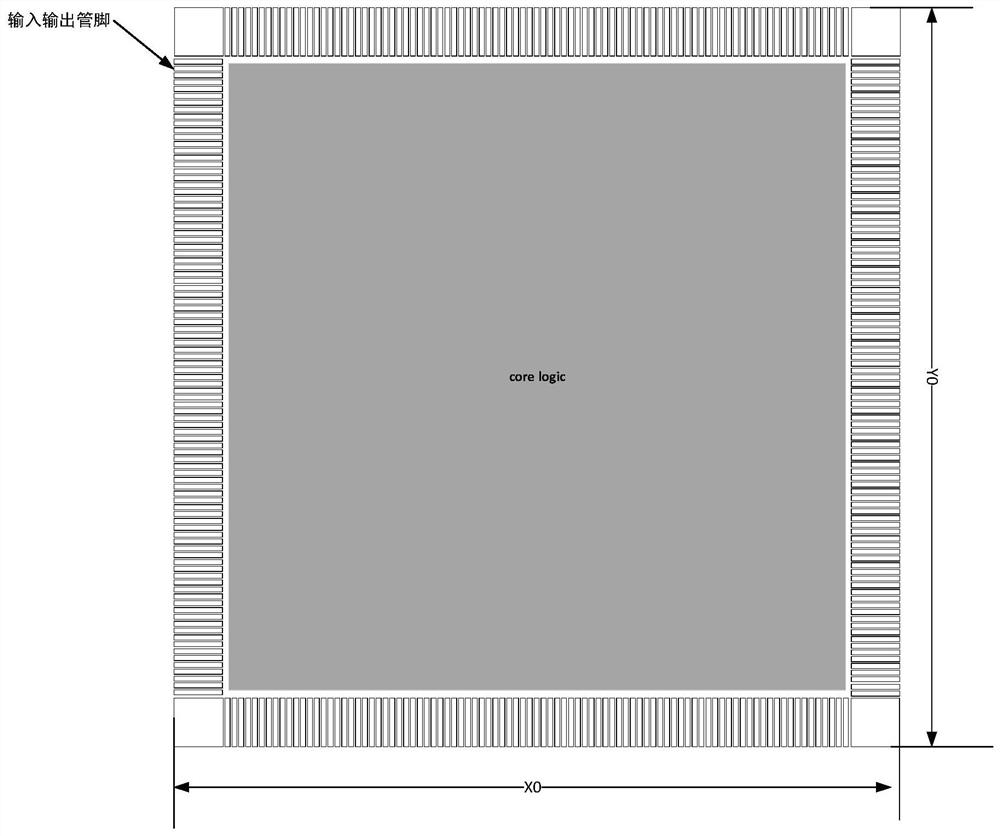
[0026] Refer to appendix 1 and appendix figure 2 , it can be seen that the arrangement of the input and output pins of the first circle and the input and output pins of the second circle of the present invention makes X1<X0, Y1<Y0, and the area of a single chip X1*Y1<X0*Y0, reaching the chip area purpose of saving.
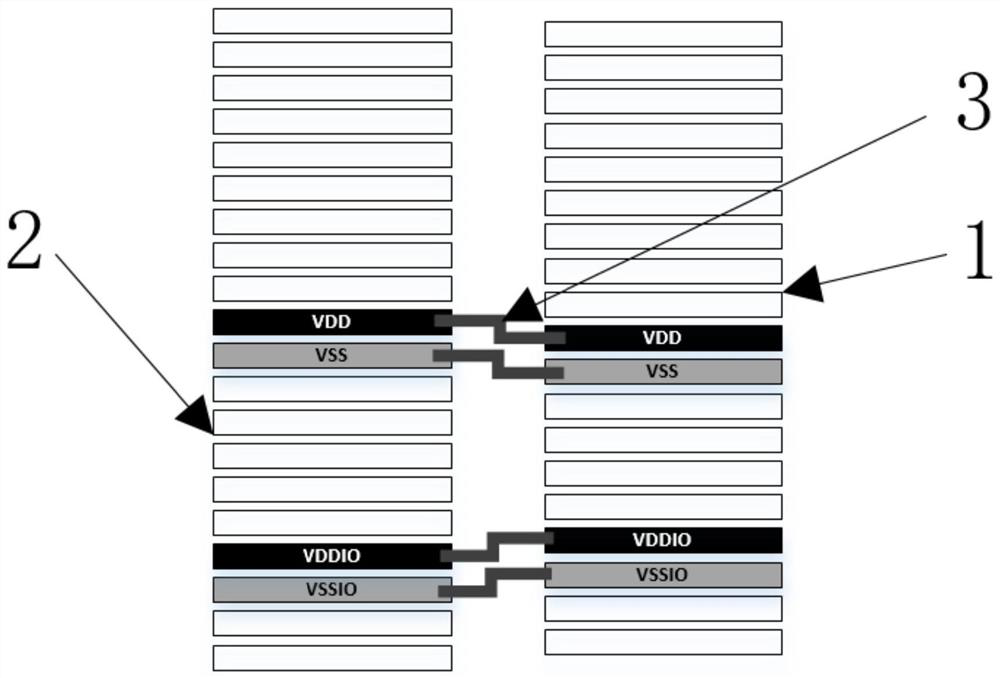
[0027] In the technical solution of the present invention, those skilled in the art know that the chip has a large number of input and output p...
Embodiment 2
[0036] On the basis of Embodiment 1, the present invention also discloses a chip, which includes core logic and input and output pins, and input and output pins are arranged around the core logic; the input and output pins include: a first circle of input and output pins Output pins, input and output pins of the second circle and input and output pins of the third circle; the core logic is arranged in the input and output pins of the first circle, and the input and output pins of the first circle are arranged in the input and output pins of the second circle In the output pins, the input and output pins of the second circle are arranged in the input and output pins of the third circle.
[0037]Combined with the connection scheme of the power ground pins in implementation 1, the power ground pins of the input and output pins of the first circle, the power ground pins of the input and output pins of the second circle, and the power ground pins of the input and output pins of the ...
Embodiment 3
[0042] On the basis of implementation 1 or implementation 2, refer to the appendix Figure 7 , those skilled in the art can set the number and position of the input and output pins of the first circle as needed, and do not necessarily completely surround the core logic; those skilled in the art can set the number and position of the input and output pins of the second circle as needed. The number and position of the pins do not necessarily completely surround the first circle of input and output pins.
PUM
 Abstract
Description
Claims
Application Information
 - R&D Engineer
- R&D Manager
- IP Professional
- Industry Leading Data Capabilities
- Powerful AI technology
- Patent DNA Extraction
Browse by: Latest US Patents, China's latest patents, Technical Efficacy Thesaurus, Application Domain, Technology Topic, Popular Technical Reports.
© 2024 PatSnap. All rights reserved.Legal|Privacy policy|Modern Slavery Act Transparency Statement|Sitemap|About US| Contact US: help@patsnap.com


