
Diodes and methods of forming them

A diode and tooth-shaped technology, applied in the field of diodes and their formation, can solve the problem of excessive wafer area occupied by diodes, and achieve the effects of saving wafer area, increasing contact area, and increasing capacitance

Active Publication Date: 2019-01-04
SHANGHAI HUAHONG GRACE SEMICON MFG CORP
View PDF4 Cites 0 Cited by
  • Summary
  • Abstract
  • Description
  • Claims
  • Application Information

AI Technical Summary

Problems solved by technology

[0005] However, the diodes in the prior art have the problem of occupying too much wafer area

Method used


Image

  • Diodes and methods of forming them
  • Diodes and methods of forming them
  • Diodes and methods of forming them

Examples


Embodiment Construction

[0027] It can be seen from the background art that the diode in the prior art has the problem of too large area. Now combine the structure of the diode in the prior art to analyze the reason of its too large area:

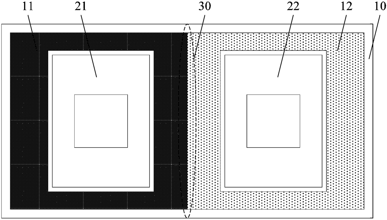
[0028] refer to figure 1 , shows a schematic diagram of a top view structure of a diode.

[0029] The diode includes a substrate 10; an N-type semiconductor layer 11 and a P-type semiconductor layer 12 adjacent to the surface of the substrate 10; The second connecting piece 22 .

[0030] The first connector 21 is connected to the metal wire (static receiving end), the second connecting member 22 is connected to the ground (static discharge end), and the potential of the metal wire is higher than the ground. Therefore, the PN junction formed by the N-type semiconductor layer 11 and the P-type semiconductor layer 12 is reverse-biased between the metal line and the ground, so the diode is in a cut-off state under normal operating conditions, and does not affect the...


PUM


Abstract

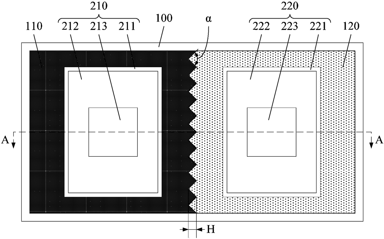
The invention provides a diode and a forming method thereof. The diode comprises a substrate, a first semiconductor layer and a second semiconductor layer, wherein the first semiconductor layer and the second semiconductor layer are arranged on the substrate adjacently. The first semiconductor layer and the second semiconductor layer are contacted to form a PN junction; the first semiconductor layer is connected with a static receiving end, the second semiconductor layer is connected with a static discharging end, and thus the PN junction is allowed to be in an anti-phase bias state; and the first semiconductor layer and the second semiconductor layer respectively have a tooth interface. The interfaces of the first semiconductor layer and the second semiconductor layer of the diode are the tooth interfaces respectively, so that contact area between the first semiconductor layer and the second semiconductor layer is increased, capacitance of the diode is increased, discharge capability of the single diode is improved, the number of the diodes can be effectively reduced, wafer area is saved, and device integration level is improved.

Description

technical field [0001] The invention relates to the field of semiconductor manufacturing, in particular to a diode and a forming method thereof. Background technique [0002] Electrostatic Discharge poses a serious threat to the reliability of integrated circuits. Moreover, with the development of semiconductor technology, the size of semiconductor devices continues to shrink, and the device density continues to increase. On the one hand, the thickness of the dielectric layer is getting thinner and thinner, and the electrostatic pressure that the device can withstand is getting lower and lower; on the other hand, it is easy to generate and accumulate Electrostatic materials (such as plastics, rubber, etc.) are widely used, which greatly increases the probability of integrated circuits being damaged by electrostatic discharge. [0003] Conductors such as metal wires or polysilicon in semiconductor devices are like antennas, which will accumulate static electricity during the...

Claims


Application Information

Patent Timeline
Patent Type & Authority Patents(China)
IPC IPC(8): H01L29/861H01L29/06H01L21/329
CPCH01L29/0688H01L29/66136H01L29/861
Inventor 曹云
Owner SHANGHAI HUAHONG GRACE SEMICON MFG CORP
Learn More