
Insulation film formation device

a technology of insulating film and forming device, which is applied in the direction of liquid surface applicators, electrostatic spraying apparatus, coatings, etc., can solve the problems of increasing the footprint of the entire sod system, generating difficulty in the sod system, and poor transfer efficiency of wafers within the sod system. achieve the effect of reducing the footprint of the insulating film-forming apparatus, reducing the transferring distance of the substrate, and high throughpu

Inactive Publication Date: 2010-03-23
TOKYO ELECTRON LTD
View PDF18 Cites 11 Cited by
  • Summary
  • Abstract
  • Description
  • Claims
  • Application Information

AI Technical Summary

Benefits of technology

The present invention provides an insulating film-forming apparatus that can reduce its footprint and improve transfer efficiency of the substrate. It includes a substrate process section for applying a prescribed processing to the substrate for forming an insulating film, a substrate transfer section for transferring the substrate from the outside into the substrate process section, and a substrate transfer mechanism for transferring the substrate between the substrate process section and the substrate transfer section. The substrate process section includes a process tower housed in a housing and consisting of a plurality of process units, which are stacked one upon the other, for performing a series of processing for forming an insulating film. The process tower has a frame of a prescribed shape and the plural process units are detachable from the frame. The apparatus also includes a unit control device for controlling the processing of the substrate in each process unit and a tower control apparatus for controlling the entire process performed by the plural process units. The apparatus can be easily maintained and has a high through-put. It also allows for the addition of a substrate process section without increasing the footprint of the apparatus. The coating unit has a two-stage structure and a waste liquid recovery section for efficient use of the chemical liquid. The apparatus also includes a chemical liquid tank for storing the chemical liquid and a pump for supplying the chemical liquid to the process unit. This reduces the waste of the chemical liquid.

Problems solved by technology

However, if a plurality of process units are arranged in a dispersed fashion as in the SOD system quoted above, the footprint of the entire SOD system is increased.
Also, the transfer efficiency of the wafer within the SOD system is rendered poor so as to lower the through-put.
Further, a difficulty is generated in the SOD system quoted above in performing various automatic controls.
If various automatic controls are to be performed on the basis of the measured data so as to change the process parameters in the coating unit and the baking unit and to generate an alarm when the thickness of the coating film exceeds a prescribed range, it is difficult to locate the process unit causing the inconvenience.
It is also difficult to supervise the entire apparatus.
Still further, where a certain process unit is in trouble, it is necessary to stop all the processing in the SOD system for coping with the process unit that is in trouble, with the result that the productivity is lowered.
Also, since the process units are arranged in a dispersed fashion in the SOD system 450, the transfer efficiency of the wafer is made poor so as to lower the through-put.
Since the chemical liquid used in the SOD system tends to be solidified, a serious problem is generated that the horizontal portion of the drain pipe 469 is plugged with the waste chemical liquid.
What should be noted in this connection is that the manufacturing process of the SOD system is made complex by the dispersion of the specification of the piping so as to give rise to the problem that the productivity is lowered.
Therefore, it is necessary to discharge as a waste material a large amount of the chemical liquid remaining inside the supply path, leading to an increased process cost.

Method used


Image

  • Insulation film formation device
  • Insulation film formation device
  • Insulation film formation device

Examples


Embodiment Construction

[0068]An embodiment of the present invention will now be described with reference to the accompanying drawings.

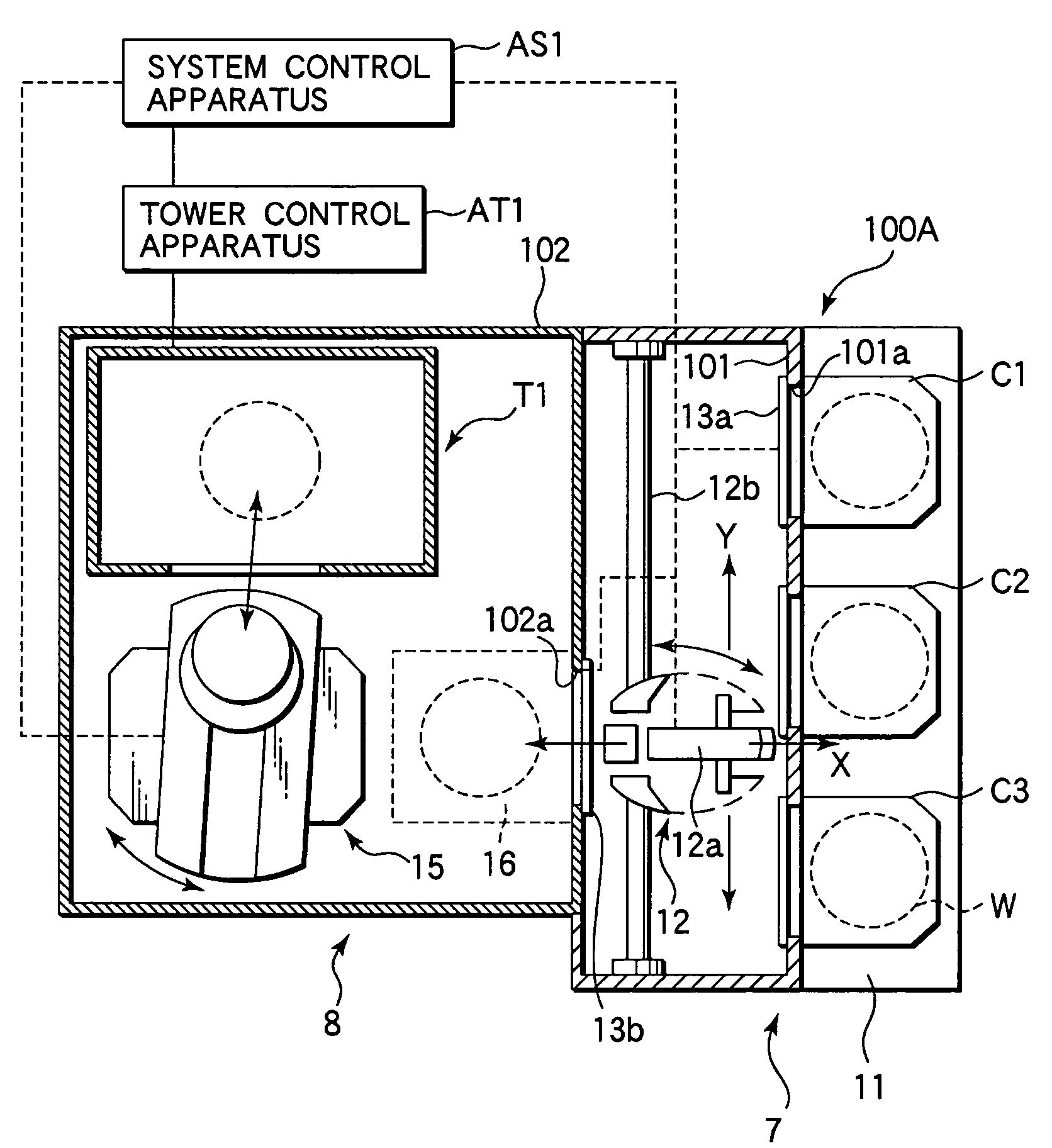
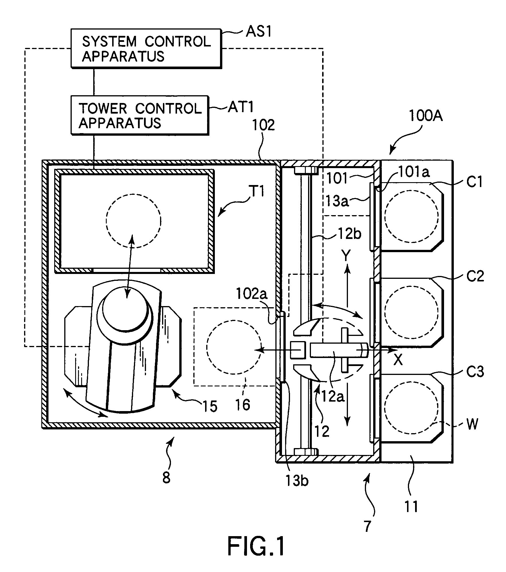
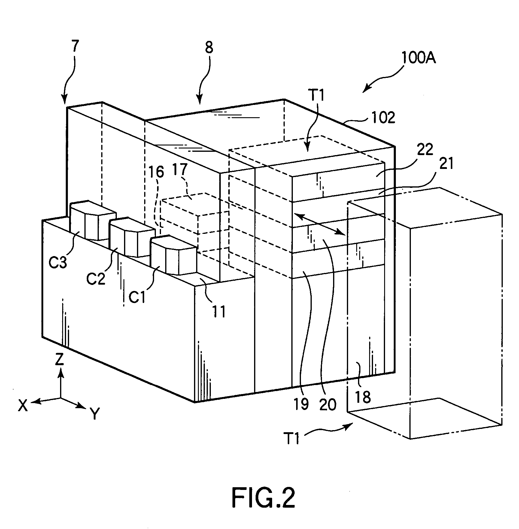
[0069]FIG. 1 is a horizontal cross sectional view schematically showing the construction of an SOD system 100A for forming an insulating film by an SOD method, and FIGS. 2 and 3 are an oblique view and a side view, respectively, each showing the construction of the SOD system 100A shown in FIG. 1.

[0070]The SOD system 100A comprises a process block 8 for applying a prescribed processing to a wafer W and a carrier block 7 for transferring the wafer W between a carrier C housing a prescribed number of wafers W and the process block 8.

[0071]The carrier block 7 includes a carrier table 11 on which a plurality of carriers, e.g., three carriers C1 to C3, can be disposed and a sub-transfer mechanism 12 for transferring the wafer W between the carriers C1 to C3 disposed on the carrier table 11 and the process block 8. The sub-transfer mechanism 12 is arranged within a housing 101.

[0...


PUM


Abstract

An SOD system (100A) comprises a process block (8) for performing a prescribed processing so as to form an insulating film on a wafer W, a carrier block (7) for transferring the wafer W from the outside into the process block (8), a sub-transfer mechanism (12) for transferring the substrate W between the process block (8) and the carrier block (7), and a main transfer mechanism (15). A process tower (T1) prepared by stacking one upon the other a plurality of process units for performing a series of processing for forming an insulating film on the wafer W is arranged detachable from the process block (8).

Description

TECHNICAL FIELD[0001]The present invention relates to an insulating film-forming apparatus for forming an insulating film on a substrate such as a semiconductor wafer or an LCD substrate (a glass substrate for a liquid crystal display).BACKGROUND ART[0002]In the manufacturing process of a semiconductor device, an SOD (Spin on Dielectric) method is employed as one of the technologies for forming an insulating film (an interlayer insulating film) on a semiconductor wafer. In the SOD method, a coating film, i.e., a film formed by the coating method, is formed on a wafer by a spin coating method, followed by applying a chemical processing or a heat processing or the like to the coating film so as to form an insulating film. To be more specific, the surface of a wafer is coated first with a chemical liquid prepared by dispersing the material for forming the insulating film in a solvent, followed by evaporating the solvent from the coating film so as to dry the coating film. Then, a bakin...

Claims


Application Information

Patent Timeline
Patent Type & Authority Patents(United States)
IPC IPC(8): H01L21/306B05B13/00B05B13/04B05C11/00H01L21/00
CPCH01L21/67017H01L21/6715H01L21/67754H01L21/67184H01L21/6719H01L21/67178
Inventor NISHIBAYASHI, TAKAHIRO
Owner TOKYO ELECTRON LTD
Learn More