Methods of fabricating semiconductor devices including channel layers having improved defect density and surface roughness characteristics
a technology of semiconductor devices and defect density, applied in semiconductor devices, semiconductor/solid-state device details, electrical devices, etc., can solve the problems of increasing the degree of integration by decreasing the size of patterns, increasing the manufacturing cost of sram devices, and reducing the number of chips manufactured on a substrate, so as to improve the surface roughness characteristics, improve the effect of quality and uniform thickness
- Summary
- Abstract
- Description
- Claims
- Application Information
AI Technical Summary
Benefits of technology
Problems solved by technology
Method used
Image

Examples
example 1
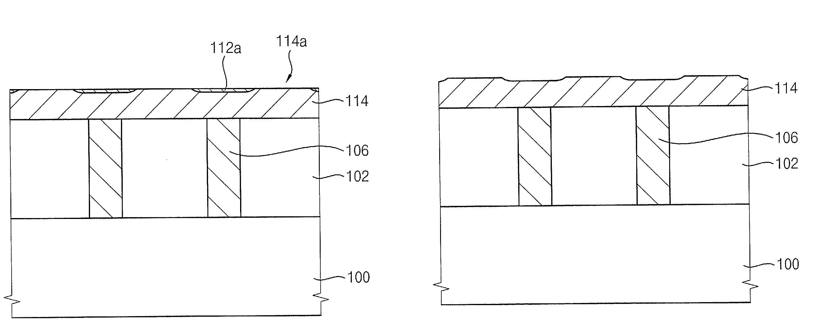
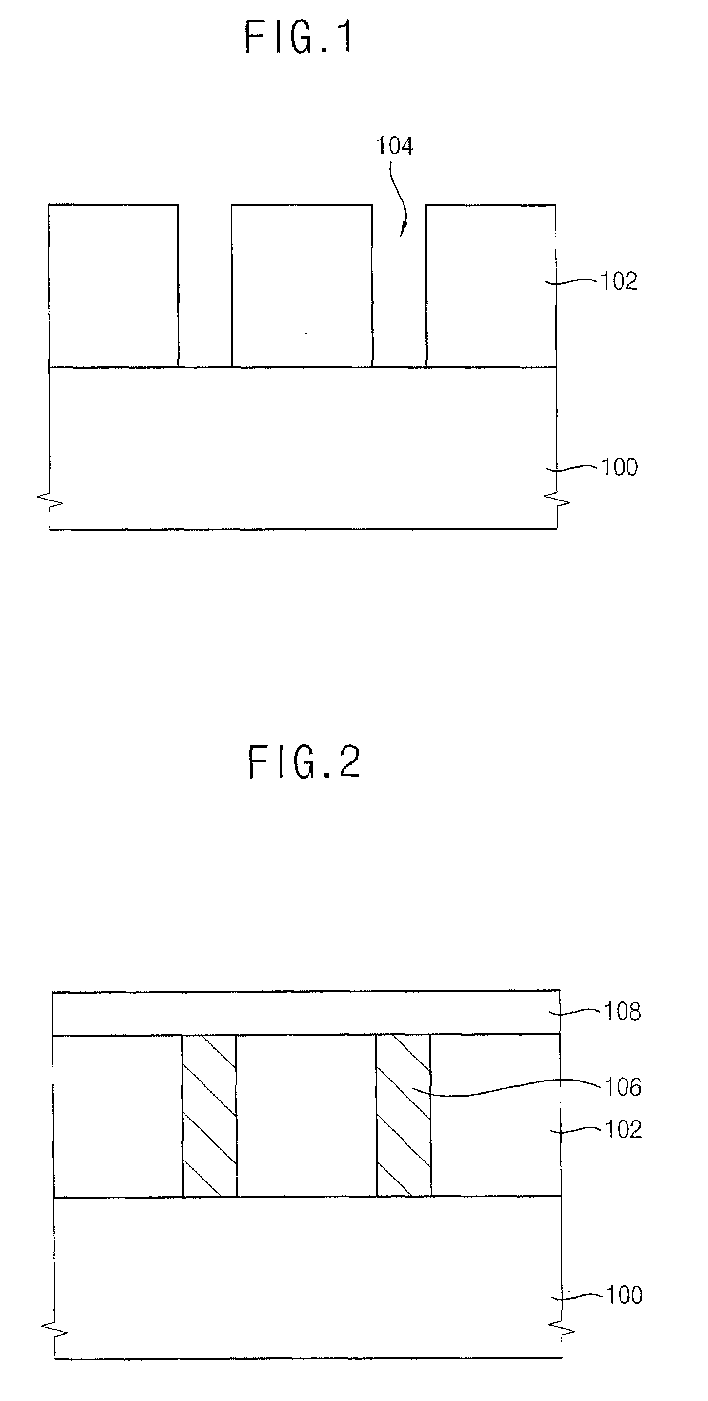
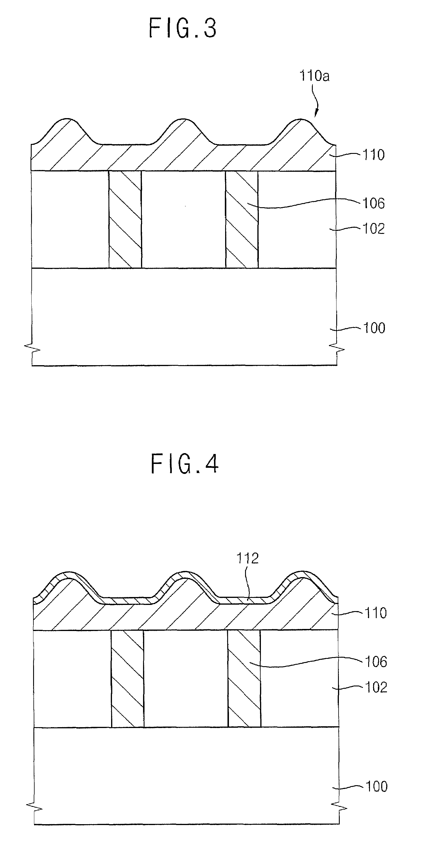
[0098]A silicon channel layer was formed on a substrate to have a thickness of about 29.5 nm, and a first transistor was formed on the silicon channel layer.
example 2
[0099]A silicon channel layer was formed on a substrate to have a thickness of about 25.9 nm, and a second transistor was formed on the silicon channel layer.
example 3
[0100]A silicon channel layer was formed on a substrate to have a thickness of about 19.6 nm, and a third transistor was formed on the silicon channel layer.
PUM
 Abstract
Description
Claims
Application Information
 - R&D
- Intellectual Property
- Life Sciences
- Materials
- Tech Scout
- Unparalleled Data Quality
- Higher Quality Content
- 60% Fewer Hallucinations
Browse by: Latest US Patents, China's latest patents, Technical Efficacy Thesaurus, Application Domain, Technology Topic, Popular Technical Reports.
© 2025 PatSnap. All rights reserved.Legal|Privacy policy|Modern Slavery Act Transparency Statement|Sitemap|About US| Contact US: help@patsnap.com