
Directly-modulated diode lasers with reduced overshoot

a diode laser and direct modulation technology, applied in the field of optical communication, can solve the problems of reducing the usefulness of a dml, reducing the efficiency of a laser, and difficult to remove all cycles, so as to reduce the overshoot on the 0 to 1 transition, improve performance, and improve performance.

Active Publication Date: 2010-02-02
LUMENTUM TECH UK LTD
View PDF2 Cites 9 Cited by
  • Summary
  • Abstract
  • Description
  • Claims
  • Application Information

AI Technical Summary

Benefits of technology

[0024]The invention provides a method of driving a direct modulated resonant cavity optoelectronic device, such as a semiconductor laser, such that it is suitable for high bit rate operation with improved performance with respect to the performance mask, and which in particular provides a method of decreasing the overshoot on the 0 to 1 transition.
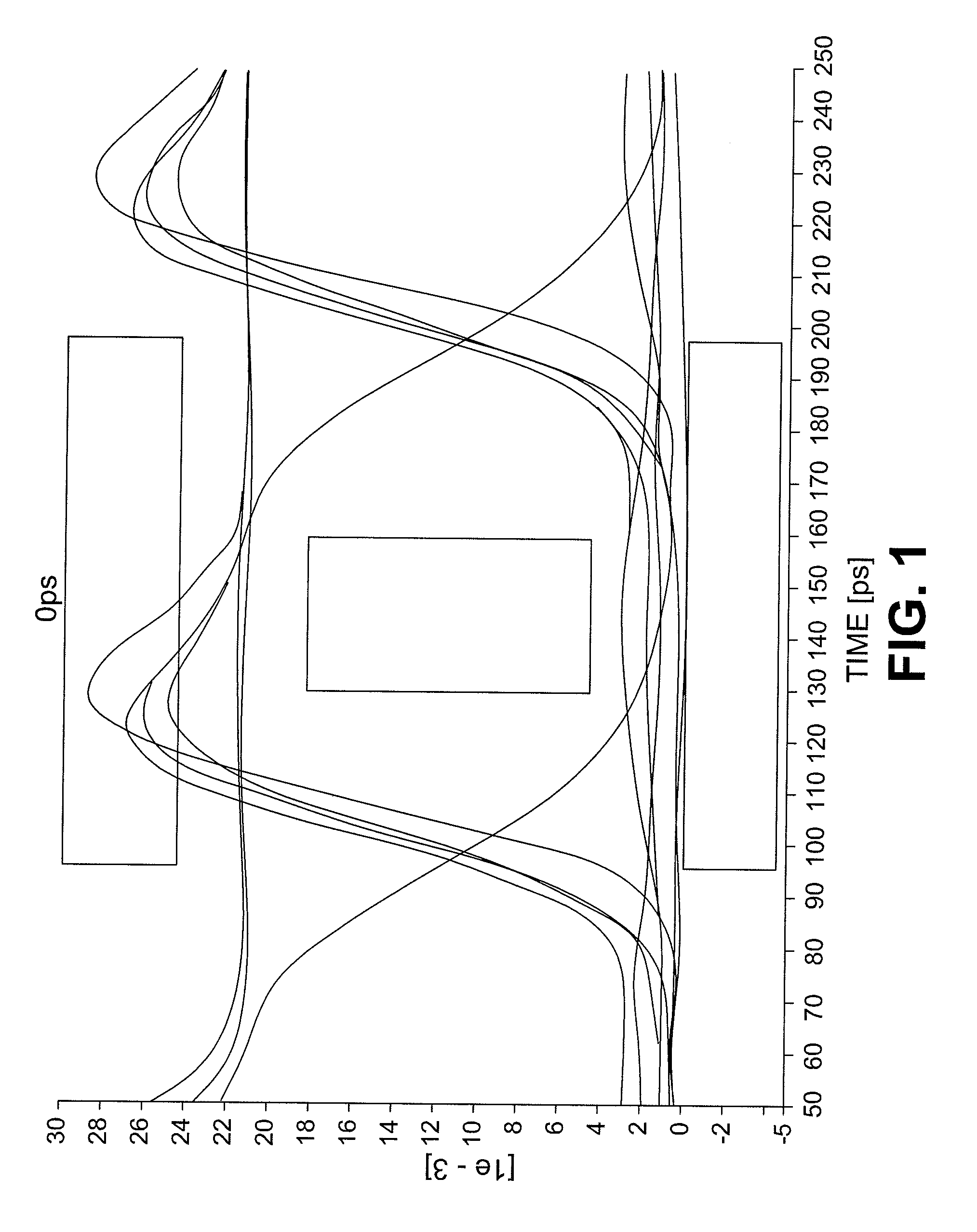
[0031]The inventive method can be used to complement other design approaches. The multi-section with fixed delay design could in principle be applied to any DFB. However, as a means of improving amplitude modulation, as illustrated by the optical eye (a measure of the quality of the amplitude modulation), of FIG. 1, it is particularly beneficial to high modulation rate systems. Below 2.5 Gb / s the benefit is likely to be small because such devices will only need to be driven with a signal that has a relatively slow rise time, so the optical intensity output of a device with a top electrode comprising only a single electrode section will follow the drive signal to an acceptable degree. With a slow rise time, the laser's optical carrier inversion will be much smaller and less significant than for a more sudden change.
[0033]Yet another aspect of the invention provides a direct modulation laser comprising a carrier; a laser chip provided on said carrier, said laser chip including an electrode divided into at least two separate electrode sections for applying respective electrical drive signals derived from a common input signal to an active region of the laser to generate components of an optical output; transmission lines on said carrier for applying the electrical drive signals to said respective electrode sections; and said transmission lines being configured to introduce a time delay between the electrical drive signal applied to one of said electrode sections and the electrical drive signal applied to the other of said electrode sections whereby the components of the optical output resulting from the drive signal applied to each section reach a peak intensity at different times to suppress amplitude overshoot and amplitude oscillation during transitions from a low to high output level.
[0034]In one embodiment the invention provides a multi-section DFB (distributed feedback) laser wherein a grating is written along the path of the optical mode to govern the lasing wavelength with a time delay between some of the driven sections. While it can be expected that each section will have a modulation response that is similar to that of a conventional single section DML, by providing a time delay between different sections of the laser, it can be ensured that the sections reach their individual peaks at different times.
[0036]In a simple embodiment the laser comprises two sections. Potentially there could be further advantages to the laser comprising more than two sections (e.g. three sections), albeit at the cost of increased manufacturing complexity.

Problems solved by technology

A major issue is overshoot on the rising edge during the transition to the logical 1 level.
This is a long-standing problem that significantly restricts the usefulness of a DML, particularly for applications involving high speed digital or analogue modulation.
At 10 Gb / s and above it is extremely difficult to remove all the cycles, and often the first cycle remains.
Damping is not an easy property to modify by design.
Unfortunately these parameters cannot be readily modified to improve the laser performance.
This degrades system performance.
It is also possible to modify the cavity coatings or grating strength (in the case of a DFB laser), but the increase in the photon density is usually small, and in the case of a larger grating strength can lead to other problems such as a decrease in the single-mode yield.
Unfortunately, reported variations in gain saturation are small and are not easily translatable into different material systems or different operating wavelengths since the fundamental physical mechanism behind gain saturation in commercial diode lasers is still not fully understood.
However, in commercial diode lasers comprising multiple quantum well (MQW) active layers the understanding of how much the carrier transport time can be varied in this way is still incomplete.
Moreover, simulations indicate that too long a transport time leads to signal patterning or inter-symbol interference (ISI) and a large increase in chirp, or frequency excursion.
This also strongly limits performance at higher bit rates, such as 20 Gbit / s or 40 Gbit / s, and longer system reaches, such as greater than 20 km at 10 Gbit / s.
However, such an approach requires very fast and special laser drivers in order to realize such waveforms.
That means that the laser driver cost would probably be too prohibitive to use.
This approach is not very attractive because it complicates significantly the packaging of the laser, requiring an optical alignment between the two laser chips.
It also significantly increases the power dissipation by the device and would be difficult to use for uncooled operation.
However, this method is only suitable for low frequency modulation because as the modulation frequency exceeds the differential carrier lifetime of the laser the modulation response of the carrier density rapidly reduces.
This will limit this approach to narrow band analogue modulation or low data rate digital modulation applications.
Thus Kaede cannot be said to teach a method of improving the quality of amplitude modulation that is relatively unimportant to the device of Kaede, and in particular Kaede does not address the phenomenon of overshoot.
This approach is difficult to implement because the necessary signal driver does not presently exist as an off-the-shelf product, and would be prohibitively expensive as a custom-made product.

Method used


Image

  • Directly-modulated diode lasers with reduced overshoot
  • Directly-modulated diode lasers with reduced overshoot
  • Directly-modulated diode lasers with reduced overshoot

Examples


Embodiment Construction

[0053]It is important to achieve high quality, low distortion amplitude modulation as well as low laser chirp when using directly modulated lasers in digital high bit rate dispersion limited systems. In such systems a low distortion amplitude waveform will produce good receiver sensitivity at low fibre reaches while the presence of low chirp will help sustain the quality of the amplitude waveform as it propagates down the fibre and experiences chromatic dispersion. In loss limited applications (where chromatic dispersion is negligible) the most important attributes of the directly modulated laser are the quality of the amplitude waveform and the launched power into the fibre. For loss limited digital applications chirp reduction, or modulated frequency excursion reduction, is not particularly important. In accordance with embodiments of the invention, a multi-section direct modulation optoelectronic device is driven in such a way as to provide improved quality of amplitude modulatio...


PUM


Abstract

An optical signal is produced from a direct modulation resonant cavity device, such as directly-modulated diode laser having an electrode divided into multiple sections. Each section is driven with an electrical waveform such that a time delay is introduced between sections so as to ensure that the different sections reach their peaks at slightly different times.

Description

CROSS REFERENCE TO RELATED APPLICATION[0001]This application claims the benefit under 35 USC 119(e) of prior U.S. application No. 60 / 890,124, filed Feb. 15, 2007, the contents of which are herein incorporated by reference.FIELD OF THE INVENTION[0002]This invention relates to the field of optical communications, and in particular to direct modulation resonant cavity devices, such as a resonant cavity light emitting diode (LED) or a direct modulation semiconductor diode laser (DML) of the Fabry-Perot type or distributed-feedback (DFB) type. Such devices are typically used for generating optical signals in communication systems.BACKGROUND OF THE INVENTION[0003]In the discussion of the prior art, reference will be made in particular to a DML, which is one type of direct modulation resonant cavity device and which is exemplary of direct modulation resonant cavity devices in general.[0004]The output of a DML must be modulated in order to generate an output signal that is capable of transm...

Claims


Application Information

Patent Timeline
IPC IPC(8): H01S3/10H01S3/00H01S3/13H01S5/12
CPCH01S5/0425H01S5/0427H01S5/12H01S5/04254H01S5/04256H01S5/06226H01P5/12H01S5/02345
Inventor REID, BENOITWATSON, CHRISTOPHER
Owner LUMENTUM TECH UK LTD
Learn More