
Device for obtaining the image and/or spectra of electron energy loss

a technology of electron energy loss and electron energy loss, which is applied in the field of devices for acquiring images and/or can solve the problems of preventing fast acquisition of electron energy loss spectra of a very large dynamic range, slow image-taking, adversely affecting the acquisition of electron energy loss spectrum, etc., and achieves the stability and precision of the two voltages.

Active Publication Date: 2010-01-05
CENT NAT DE LA RECHERCHE SCI +1
View PDF6 Cites 23 Cited by
  • Summary
  • Abstract
  • Description
  • Claims
  • Application Information

AI Technical Summary

Benefits of technology

[0016]By means of these provisions, the dynamic range of the sensor can be increased by causing the exposure time of the various photosensitive portions to vary. In addition, the exposures and reads of the various photosensitive zones of the image sensor make it possible to sense the image of various portions of an energy loss spectrum, it being possible for the image to be taken continuously.
[0024]By means of these provisions, the signal-to-noise ratio of the device is improved for the photosensitive zones that are read slowest.
[0027]Thus, the response time of the deflection is negligible relative to the exposure times used for recording the various portions of the spectrum. It is thus possible to prevent the detector from recording a blur or streak due to the spectrum going past during the movements of the beam from one photosensitive zone to the other.
[0029]Thus, fast switching is implemented while also maintaining the stability and the precision of the two voltages.

Problems solved by technology

All of these operations require the image-taking to be slow, which adversely affects acquisition of an electron energy loss spectrum and, in particular, prevents fast acquisition of electron energy loss spectra of very large dynamic range.
In addition, prior art devices require the power source to remain stable (100,000 to 1,000,000 volts) for one minute, or even longer, making them vulnerable to the slightest variations in power supply voltage.
Finally, prior art devices do not make it possible to obtain high precision in positioning the energy peak, which precision is necessary for identifying the characteristic distributions in the energy loss spectrum.

Method used


Image

  • Device for obtaining the image and/or spectra of electron energy loss
  • Device for obtaining the image and/or spectra of electron energy loss
  • Device for obtaining the image and/or spectra of electron energy loss

Examples


Embodiment Construction

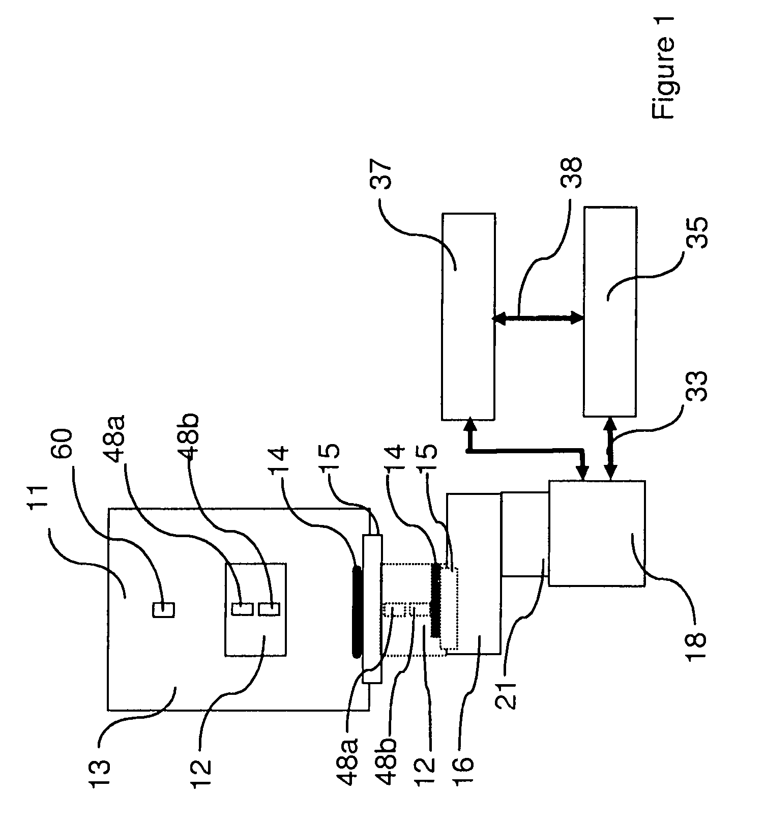
[0040]The device 10 of the present invention whose structure is shown in FIG. 1 is used to form images in High-Speed (HS) mode or in High-Resolution (HR) mode, and to detect the electrons of an energy loss spectrum that are formed on an electron microscope 11 equipped with a spectrometer 12 disposed in or at the outlet of the column 13 of the electron microscope 11. The electron-photon conversion is performed by a scintillator 14 placed on a view port 15 which also provides vacuum-tightness.

[0041]Optical transfer means 16 make it possible to re-form an identical image on the sensitive portion of a CCD image sensor 17. This image sensor 17 is located in a detection head 21 (see FIG. 2) and it is cooled to in the range −30° C. to −60° C. depending on needs, i.e. depending on the exposure times that are necessary. For example, the image sensor is a commercially available product referenced ATMEL TH7899M that has 2084×2048 pixels of 14×14 μm. It is of the full frame transfer type and it...


PUM


Abstract

The inventive device for obtaining the electron energy loss image and / or spectra includes an image sensor, a control for at least two deflectors for alternately exposing at least two photosensitive parts of the image sensor, sensor reading means for generating the representative signal of an image captured by each photosensitive part of the image sensor, means for synchronizing the deflector and the reading means for successively controlling the exposition of the photosensitive part and the reading of the other photosensitive part for each photosensitive part and means for combining the two image parts in such a way that a spectrum is formed.

Description

CROSS-REFERENCE TO RELATED APPLICATIONS[0001]This application is a National Phase Application of PCT / EP2005 / 053745, which claims priority to FR 0408633, which is hereby incorporated by reference.FIELD OF THE INVENTION[0002]The present invention relates to a device for acquiring images and / or electron energy loss spectra. It applies in particular to acquiring images in multimode mode (high-speed mode and high-resolution mode) and to fast acquisition of electron energy loss spectra of very large dynamic range.BACKGROUND OF THE INVENTION[0003]Changes in the needs of laboratories who use electron microscopes as investigation tools, and in particular changes in themes towards studying materials at nanometric scale are requiring increasingly high-performance investigation means. In electron microscopy, the techniques used are changing towards quantitative use of images, requiring acquisition methods to be developed.[0004]An electron energy loss spectrum is made up mainly of two zones, nam...

Claims


Application Information

Patent Timeline
IPC IPC(8): H01J37/28H01J37/244H01J37/256
CPCH01J37/244H01J37/256H01J2237/2522
Inventor PINNA, HENRITENCE, MARCEL
Owner CENT NAT DE LA RECHERCHE SCI
Learn More