Method of manufacturing thin film transistor, thin film transistor, and display unit
a technology of thin film transistors and display units, which is applied in the direction of transistors, solid-state devices, semiconductor devices, etc., can solve the problems of reducing on-characteristics, generating unnecessary compounds, and destroying the crystalline silicon film forming the channel region
- Summary
- Abstract
- Description
- Claims
- Application Information
AI Technical Summary
Benefits of technology
Problems solved by technology
Method used
Image
Examples
first embodiment
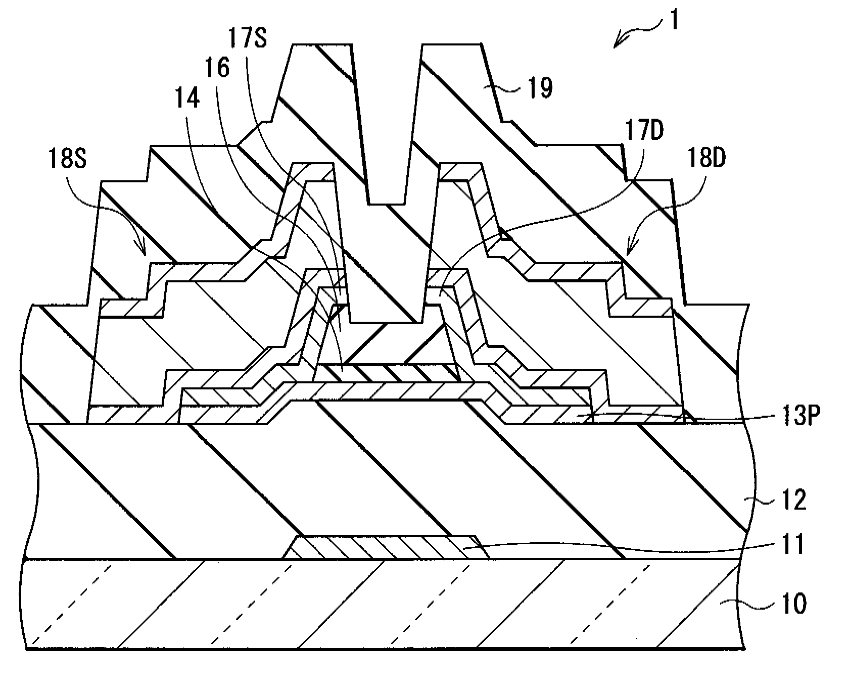
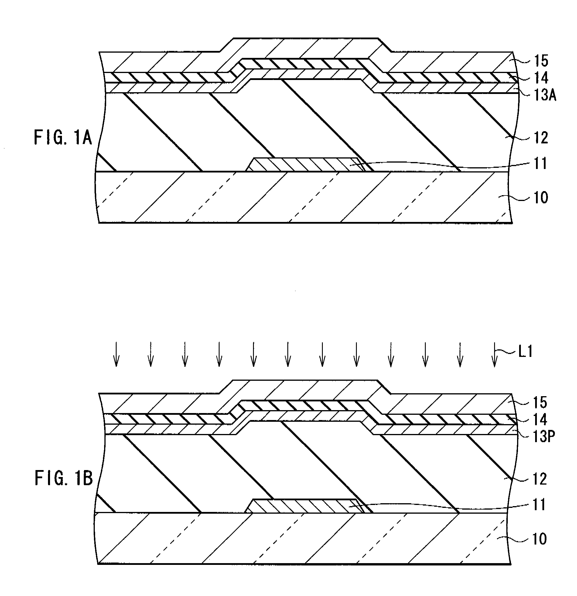
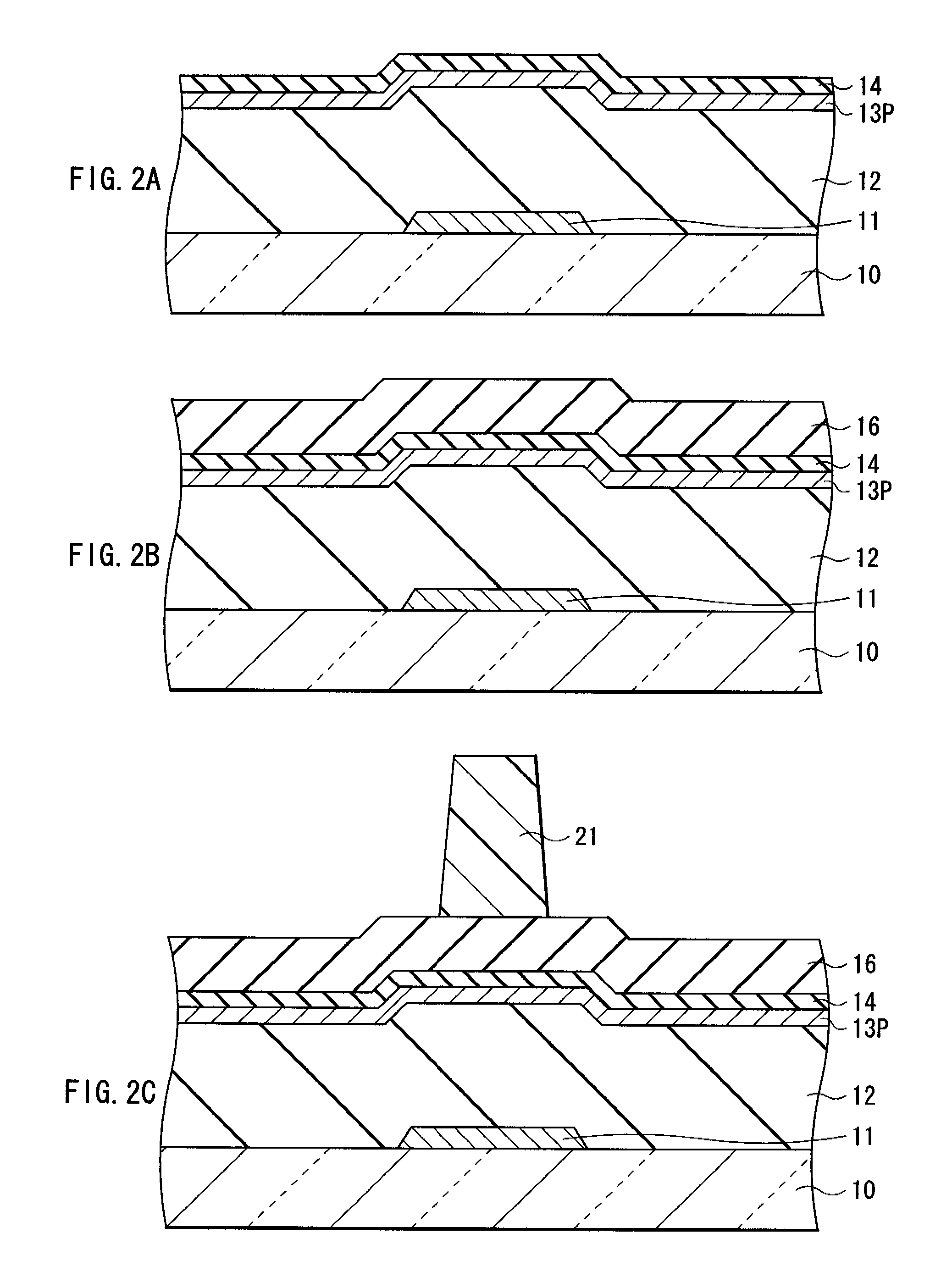
[0041]FIG. 1A to FIG. 5B are views for explaining a method of manufacturing a thin film transistor (thin film transistor 1) according to a first embodiment of the invention.
[0042]First, as shown in FIG. 1A, a gate electrode 11, a gate insulating film 12, an amorphous silicon film 13A (first amorphous silicon film), a buffer layer 14 (first insulating film), and a photothermal conversion layer 15 are formed in this order over an insulative substrate 10 made of a glass material and a plastic material.
[0043]More specifically, the gate electrode 11 is formed as follows. A molybdenum (Mo) film being about 100 nm thick is uniformly formed on the substrate 10 by, for example, sputtering method. After that, the molybdenum film is etched and patterned in a given shape. The patterning into such a given shape is made by, for example, photolithography method or the like. The gate electrode 11 is not necessarily made of Mo, but may be made of a metal with the high melting point that is hardly al...
second embodiment
[0066]Next, a description will be given of a method of manufacturing a thin film transistor (thin film transistor 1A) according to a second embodiment of the invention. Elements identical with the elements in the first embodiment are affixed with the identical symbol, and the description thereof will be omitted as appropriate.
[0067]First, as shown in FIG. 10A, in the same manner as in the thin film transistor 1 of the first embodiment, the gate electrode 11, the gate insulating film 12, the amorphous silicon film 13A, the buffer layer 14, and the photothermal conversion layer 15 are sequentially formed over the substrate 10. Next, the photothermal conversion layer 15 is uniformly irradiated with the laser beam L1, and heat treatment is indirectly provided for the amorphous silicon film 13A, and thereby the crystalline silicon film 13P is formed. Next, in the same manner as in the thin film transistor 1, the buffer layer 14 and the insulating film 16 are patterned to form the channel...
PUM
| Property | Measurement | Unit |
|---|---|---|
| thickness | aaaaa | aaaaa |
| thick | aaaaa | aaaaa |
| thick | aaaaa | aaaaa |
Abstract
Description
Claims
Application Information
 - R&D Engineer
- R&D Manager
- IP Professional
- Industry Leading Data Capabilities
- Powerful AI technology
- Patent DNA Extraction
Browse by: Latest US Patents, China's latest patents, Technical Efficacy Thesaurus, Application Domain, Technology Topic, Popular Technical Reports.
© 2024 PatSnap. All rights reserved.Legal|Privacy policy|Modern Slavery Act Transparency Statement|Sitemap|About US| Contact US: help@patsnap.com


