Light emitting element and light emitting device
a technology of light emitting device and light emitting element, which is applied in the direction of discharge tube luminescnet screen, transportation and packaging, and natural mineral layered products, etc., can solve the problems of image quality degradation and possible deterioration of light emitting element in light emitting device, and achieve shorter peak wavelength of emission spectrum, and light reflects more easily
- Summary
- Abstract
- Description
- Claims
- Application Information
AI Technical Summary
Benefits of technology
Problems solved by technology
Method used
Image
Examples
embodiment mode 1
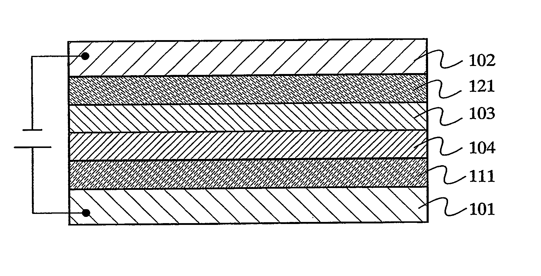
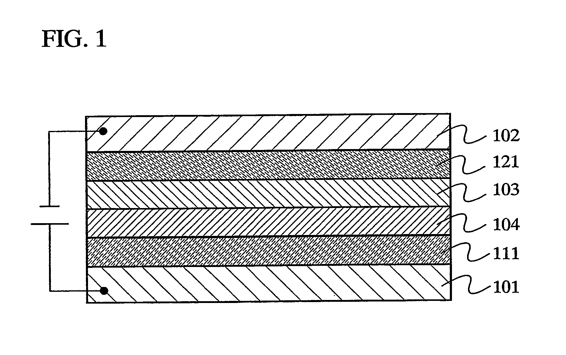
[0025]In FIG. 1, a first layer 103 containing a substance that transports holes easily and a substance with an electron accepting property and a second layer 104 containing a substance that transports electrons easily and a substance with an electron donating property are provided between a first electrode 101 and a second electrode 102. The first layer 103 and the second layer 104 are laminated in contact with each other. Further, holes are generated in the first layer 103 containing the substance that transports holes easily and the substance with the electron accepting property whereas electrons are generated in the second layer 104 containing the substance that transports electrons easily and the substance with the electron donating property.
[0026]Also, a first light emitting layer 111 is provided between the first electrode 101 and the first layer 103. A second light emitting layer 121 is provided between the second electrode 102 and the second layer 104.
[0027]Further, in this ...
embodiment mode 2
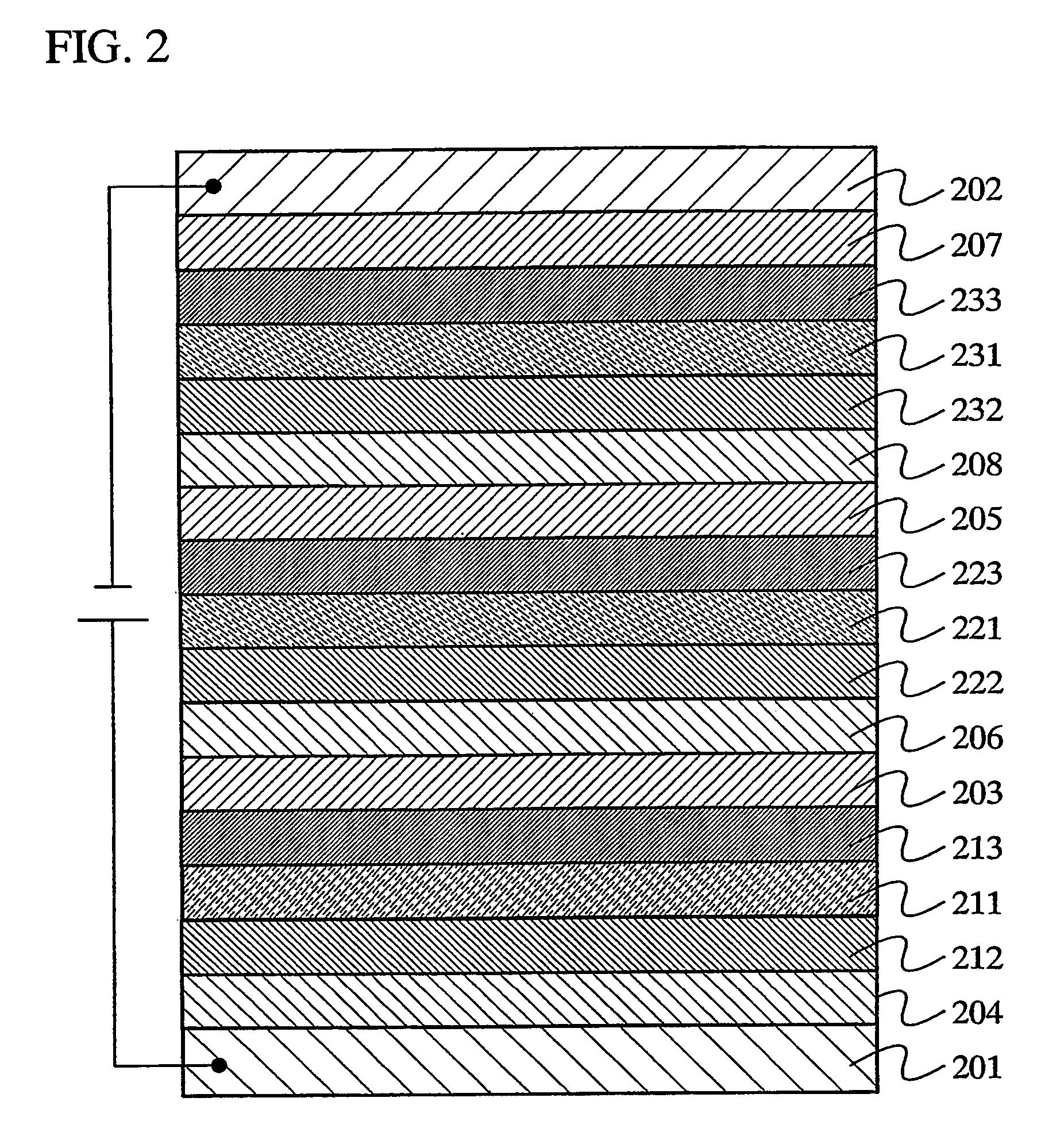
[0040]The present embodiment mode will describe a light emitting element of the invention including three light emitting layers with reference to FIG. 2.
[0041]In FIG. 2, first layers 203, 205 and 207 including a substance that transports electrons easily and a substance with an electron donating property, and second layers 204, 206 and 208 including a substance that transports holes easily and a substance with an electron accepting property are provided between a first electrode 201 and a second electrode 202. In this case, the first layer 203 is formed in contact with the first electrode 201. The second layer 208 is formed in contact with the second electrode 202. The first layer 205 and the second layer 204 are laminated to be in contact with each other. The first layer 207 and the second layer 206 are laminated to be in contact with each other. Holes are generated in the first layers 203, 205 and 207 including the substance that transports holes easily and the substance with the ...
embodiment mode 3
[0050]The light emitting element of the invention as described in Embodiment Mode 1 or 2 can be applied to a pixel portion of a light emitting device having a display function or a lighting portion of a light emitting device having a lighting function.
[0051]The present embodiment mode will describe a circuit configuration of a light emitting device having a display function and a method for driving thereof with reference to FIGS. 3 to 6.
[0052]FIG. 3 is a schematic view seen from a top face of the light emitting device according to the invention. In FIG. 3, a pixel portion 6511, a source signal line driver circuit 6512, a writing gate signal line driver circuit 6513 and an erasing gate signal line driver circuit 6514 are provided over a substrate 6500. The source signal line driver circuit 6512, the writing gate signal line driver circuit 6513 and the erasing gate signal line driver circuit 6514 are connected to FPCs (flexible printed circuits) 6503 that are external input terminals ...
PUM
| Property | Measurement | Unit |
|---|---|---|
| size | aaaaa | aaaaa |
| wavenumbers | aaaaa | aaaaa |
| pressure | aaaaa | aaaaa |
Abstract
Description
Claims
Application Information
 - R&D
- Intellectual Property
- Life Sciences
- Materials
- Tech Scout
- Unparalleled Data Quality
- Higher Quality Content
- 60% Fewer Hallucinations
Browse by: Latest US Patents, China's latest patents, Technical Efficacy Thesaurus, Application Domain, Technology Topic, Popular Technical Reports.
© 2025 PatSnap. All rights reserved.Legal|Privacy policy|Modern Slavery Act Transparency Statement|Sitemap|About US| Contact US: help@patsnap.com


