
Semiconductor device assemblies and packages including multiple semiconductor device components

a technology of semiconductor devices and components, applied in semiconductor devices, semiconductor/solid-state device details, electrical devices, etc., can solve the problems of large footprint devices, large size of devices, and inconvenient placement of semiconductor devices, so as to reduce the interposer area required for connection, reduce the thickness of the package, and facilitate the positioning of one or more semiconductor devices.

Inactive Publication Date: 2009-08-11
MICRON TECH INC
View PDF50 Cites 122 Cited by
  • Summary
  • Abstract
  • Description
  • Claims
  • Application Information

AI Technical Summary

Benefits of technology

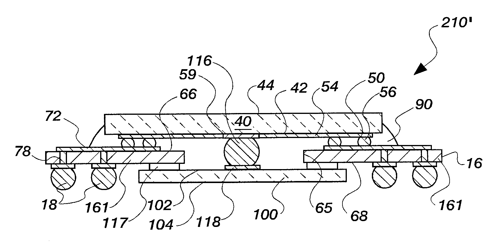
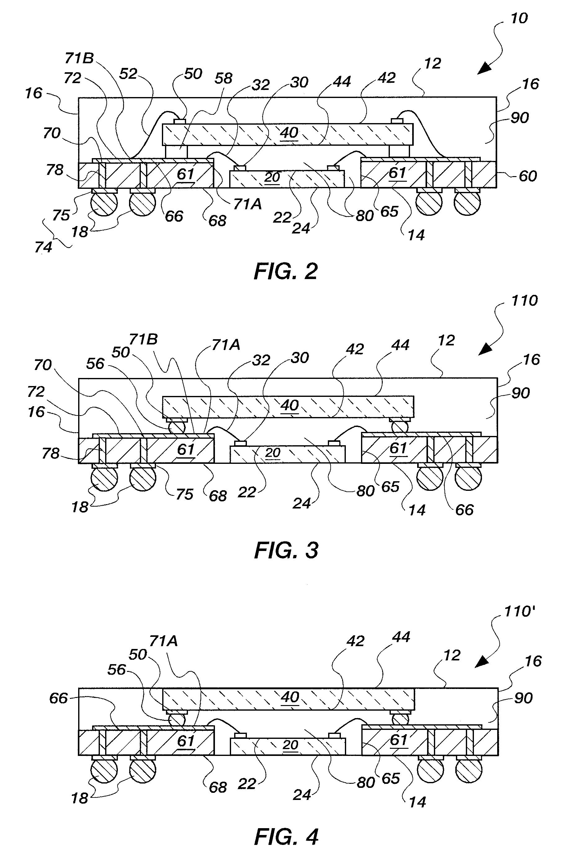
[0017]A “second-level” (e.g., upper) semiconductor device is at least partially superimposed relative to the interposer and generally to the first-level semiconductor device(s) within the interposer receptacle. The second-level semiconductor device may have its active surface facing upwardly, with its bond pads electrically connected to corresponding contact areas on the upper surface of the interposer by way of somewhat laterally extending intermediate conductive elements. Alternatively, peripheral contact areas on the second-level semiconductor device may be flip-chip bonded to contact areas on the interposer. If the first-level semiconductor device is flip-chip connected to corresponding contact areas on the active surface of the second-level semiconductor device, the active surfaces of the first- and second-level semiconductor devices face each other. Conductive traces and vias extend from the conductive areas on the interposer to corresponding outer connectors on the interposer, which are arranged in an array over the lower surface of the interposer. For small footprint packages, microvias having a diameter as small as 50 microns or smaller may be used and may be directly attached to bond pads or solder ball contact areas, for example, greatly decreasing the interposer area required for connections within a package.
[0018]Optionally, a structure such as a film or tape (e.g., a pressure-sensitive, adhesive-coated film) may be positioned on the lower side of the interposer to cover the receptacle opening, thereby closing off the bottom end of the receptacle to facilitate the positioning of one or more semiconductor devices within the receptacle. The film may be removably secured to the interposer, thereby facilitating the removal of the film following attachment of the second semiconductor device or an encapsulation process. Thus, a further reduction in the thickness of the package may be achieved.

Problems solved by technology

As with the flat packages, conventional flip-chip type packages are often undesirably thick for use in small, thin, state of the art electronic devices.
Furthermore, use of this general construction method for producing a stacked multichip module (MCM) results in a relatively high-profile, large footprint device.
While interposers that include recesses for partially receiving semiconductor devices facilitate the fabrication of thinner flip-chip type packages, the semiconductor dice of these packages, as well as intermediate conductive elements that protrude beyond the outer surfaces of either the semiconductor dice or the interposers, undesirably add to the thicknesses of these packages.
While this method results in a very low-profile flip-chip type package, the package cannot be tested separately from the carrier substrate.
As a result, if the package is unreliable, it may also be necessary to discard the carrier substrate and any other components thereon.
Moreover, the packaging method of the '695 patent complicates the process of connecting semiconductor devices and other electronic components to a carrier substrate.
In addition, it should be noted that in order to obtain a low-profile package, it may be necessary to sacrifice footprint compactness.

Method used


Image

  • Semiconductor device assemblies and packages including multiple semiconductor device components
  • Semiconductor device assemblies and packages including multiple semiconductor device components
  • Semiconductor device assemblies and packages including multiple semiconductor device components

Examples


Embodiment Construction

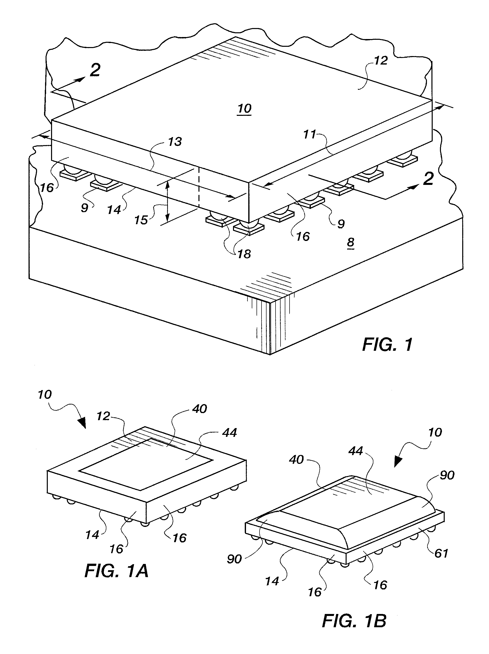
[0054]Referring to FIG. 1, a multichip semiconductor device package 10 according to the present invention is illustrated. As shown, FIG. 1 is an external view of the package 10 and is representative of a large number of possible device configurations exemplified in the figures following FIG. 1. Package 10 is illustrated as having an upper surface 12, a lower surface 14, and peripheral edges 16. Outer connectors 18, shown here as solder balls in a ball grid array (BGA) connection pattern, are depicted as being on the lower surface 14 of the package 10 and attached to contact areas 9 on a representative carrier substrate 8. The dimensions of the package 10 include length 11, width 13 and thickness 15 (exclusive of the distance outer connectors 18 protrude from the lower surface 14). The outline of the encapsulated package 10, comprising length 11 and width 13 dimensions, defines the “footprint” of the package 10. The package 10 shown in FIG. 1 represents a multidie package which has b...


PUM


Abstract

A multidie semiconductor device assembly or package includes an interposer comprising a substrate with at least one receptacle therethrough. A plurality of semiconductor device components (e.g., semiconductor devices) may be assembled with the interposer. For example, at least one contact pad of a semiconductor device component adjacent to one surface of the interposer may be electrically connected to a corresponding contact pad of another semiconductor device component positioned adjacent to an opposite surface of the interposer. As another example, multiple semiconductor device components may be at least partially superimposed relative to one another and at least partially disposed within a receptacle of the interposer.

Description

CROSS-REFERENCE TO RELATED APPLICATION[0001]This application is a continuation of application Ser. No. 10 / 184,340, filed Jun. 27, 2002, now U.S. Pat. No. 6,906,415, issued Jun. 14, 2005, which claims priority under 35 U.S.C. § 119 to Singapore patent application SG2002 / 000003684, filed on Jun. 18, 2002.TECHNICAL FIELD[0002]The present invention relates generally to stacked semiconductor device assemblies and packages, as well as to associated assembly and packaging methods. More particularly, the invention pertains to multidie assemblies and packages with low profiles and minimal size.BACKGROUND OF THE INVENTION[0003]The dimensions of many different types of state of the art electronic devices are ever decreasing. To reduce the dimensions of electronic devices, the structures by which the microprocessors, memory devices, other semiconductor devices, and other electronic components of these devices are packaged and assembled with carriers, such as circuit boards, must become more com...

Claims


Application Information

Patent Timeline
Patent Type & Authority Patents(United States)
IPC IPC(8): H01L23/52H01L23/48H01L29/40H01L23/31H01L25/065H01L25/10
CPCH01L23/3128H01L25/105H01L25/0657H01L24/97H01L2924/15151H01L2224/16145H01L2224/16225H01L2224/48091H01L2224/48227H01L2224/73257H01L2225/0651H01L2225/06513H01L2225/06524H01L2225/06527H01L2225/06541H01L2225/06555H01L2225/06586H01L2924/01079H01L2924/09701H01L2924/15311H01L2924/18161H01L2924/18165H01L2224/97H01L2225/1058H01L24/48H01L2924/01087H01L2225/1023H01L2225/1035H01L2924/00014H01L2224/81H01L2924/181H01L2924/12042H01L2224/05573H01L2224/05568H01L2224/05624H01L2224/05639H01L2224/05644H01L2924/15173H01L2224/0615H01L24/05H01L2924/00H01L2924/00012H01L2224/45099H01L2224/45015H01L2924/207
Inventor JIANG, TONGBIFEE, SETHO SINGYEAN, TAY WUUCHYE, LIM THIAM
Owner MICRON TECH INC
Learn More