DRAM memory with vertically arranged selection transistors

Inactive Publication Date: 2005-03-17
QIMONDA
View PDF5 Cites 19 Cited by
  • Summary
  • Abstract
  • Description
  • Claims
  • Application Information

AI Technical Summary

Benefits of technology

[0011] It is, therefore, the object of the invention to provide a memory cell and a method for producing memory cells, where the area required by the memory cell is further reduced and a rapid storage and read-out of digital information is made possible. Furthermore, it is the object of the invention to provide an arrangement of memory cells which permits a high packing density of the memory cells.

Problems solved by technology

The known cell arrangement has the disadvantage that a relatively large amount of area is needed for forming the memory cell.

Method used


Image

  • DRAM memory with vertically arranged selection transistors
  • DRAM memory with vertically arranged selection transistors
  • DRAM memory with vertically arranged selection transistors

Examples


Embodiment Construction

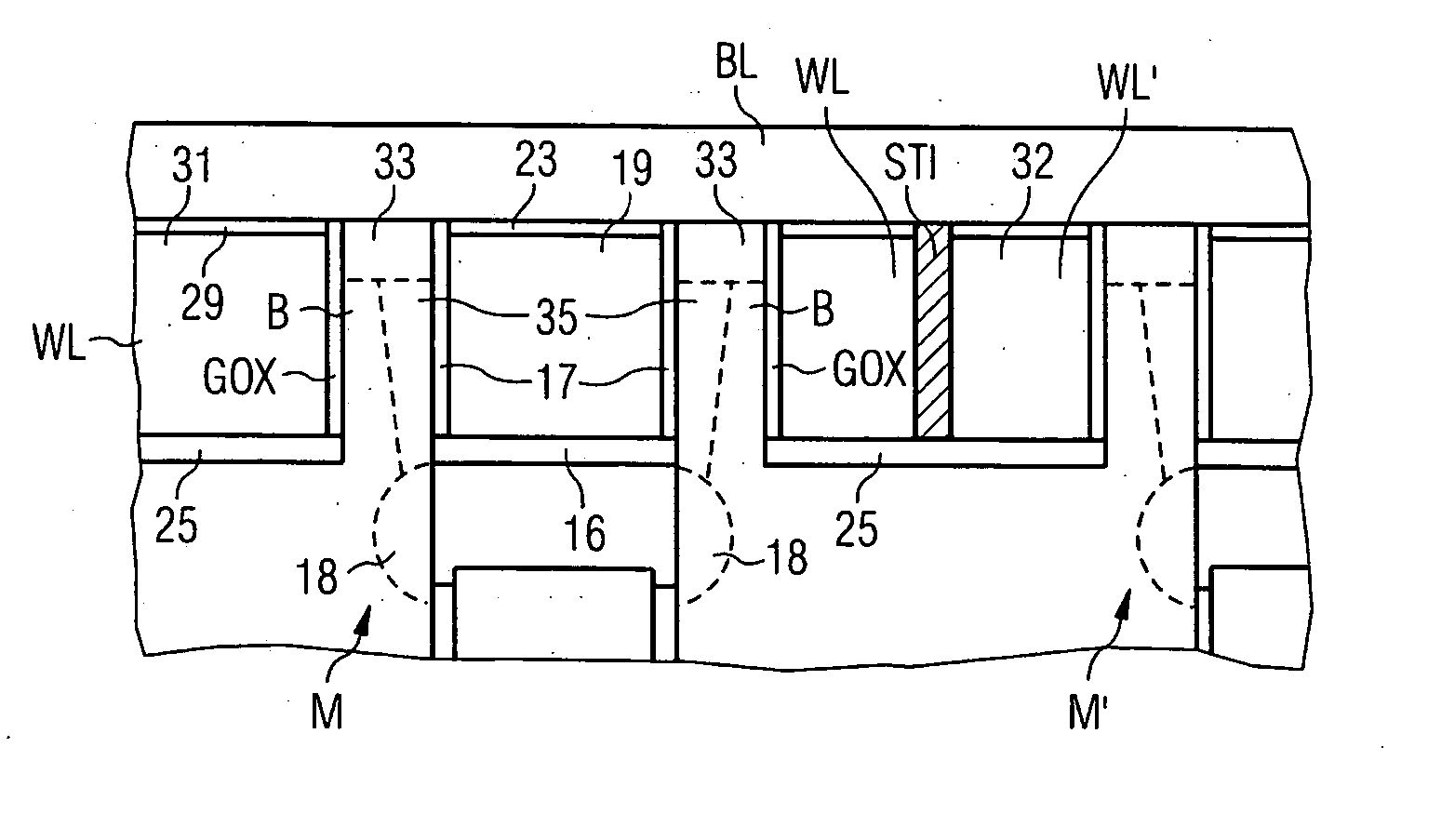
[0026]FIG. 1 diagrammatically shows the structure of a memory cell M according to the invention. To illustrate the structure, a trench hole DT with a round cross sectional area Q is shown in a perspective view. In the lower part of the trench hole DT, a trench capacitor TC is formed, the outer electrode 9 of which is preferably formed by a diffusion region (not shown here) and the inner electrode 11 of which is formed by an inner filling of the trench hole DT. The outer and the inner electrode 11, 9 of the trench capacitor TC are electrically insulated from one another by a dielectric layer 10. This layer 10 is preferably formed as an oxide layer along the cylindrical side wall of the trench hole DT and at the bottom of the trench hole DT. As shown in FIG. 1, the storage dielectric 10 extends from the trench hole bottom to about ⅔ of the trench hole height. Due to the highly diagrammatic representation of FIG. 1, the relations and distances shown therein are not reproduced true to t...


PUM


Abstract

The invention relates to a semiconductor memory, particularly a DRAM, in which the memory cells in each case have a trench capacitor arranged in a lower area of a trench hole and a vertical selection transistor which is formed adjoining an upper area of the trench hole and which connects an inner electrode of the trench capacitor to a bit line, a conductive channel being capable of being formed in dependence on the potential of a word line in the channel area, the channel area completely enclosing the trench hole in its upper area, and the associated word line at least partially enclosing the channel area.

Description

CROSS-REFERENCE TO RELATED APPLICATIONS [0001] This application claims foreign priority benefits under 35 U.S.C. §119 to co-pending German patent application number 102 60 769.9-33, filed Dec. 23, 2002. This related patent application is herein incorporated by reference in its entirety.BACKGROUND OF THE INVENTION [0002] 1. Field of the Invention [0003] The invention relates to a memory cell having a vertical selection transistor, to an arrangement of such memory cells and to a method for producing these memory cells. [0004] 2. Description of the Related Art [0005] Information can be stored and read out again with the aid of rewritable semiconductor memories. In the case of a DRAM semiconductor memory, the information is stored in the form of a particular charge in a storage capacitor. In this arrangement, each DRAM memory cell comprises one trench capacitor and one selection transistor. In the trench capacitor, a charge is stored which represents the information to be stored. The se...

Claims


Application Information

Patent Timeline
IPC IPC(8): H01L21/20H01L21/334H01L21/8242H01L27/108H01L29/76H01L31/119
CPCH01L27/10841H01L29/66181H01L27/10891H01L27/10864H10B12/395H10B12/0383H10B12/488
Inventor SOMMER, MICHAELENDERS, GERHARD
Owner QIMONDA
Why Eureka
Try Eureka