
Laser source with broadband spectrum emission

a laser source and broadband spectrum technology, applied in the direction of laser details, optical resonator shape and construction, electrical apparatus, etc., can solve the problems of low output power, low efficiency, and device size that is usually not very compact, and achieve the effect of simple fabrication

Active Publication Date: 2009-06-30
INNOLUME
View PDF101 Cites 9 Cited by
  • Summary
  • Abstract
  • Description
  • Claims
  • Application Information

AI Technical Summary

Benefits of technology

[0015]The present invention discloses a compact and inexpensive laser device, simple to fabricate, capable of emitting a broadband (preferably at least 15 nm) spectrum at a high-power level (preferably at least 100 mW and more preferably at least 150 mW, which corresponds to 10 mW per 1 nm). This combination of parameters makes such a laser device useful as an optical source for WDM-systems, and replaces a number of complex and expensive lasers, e.g. tunable lasers.

Problems solved by technology

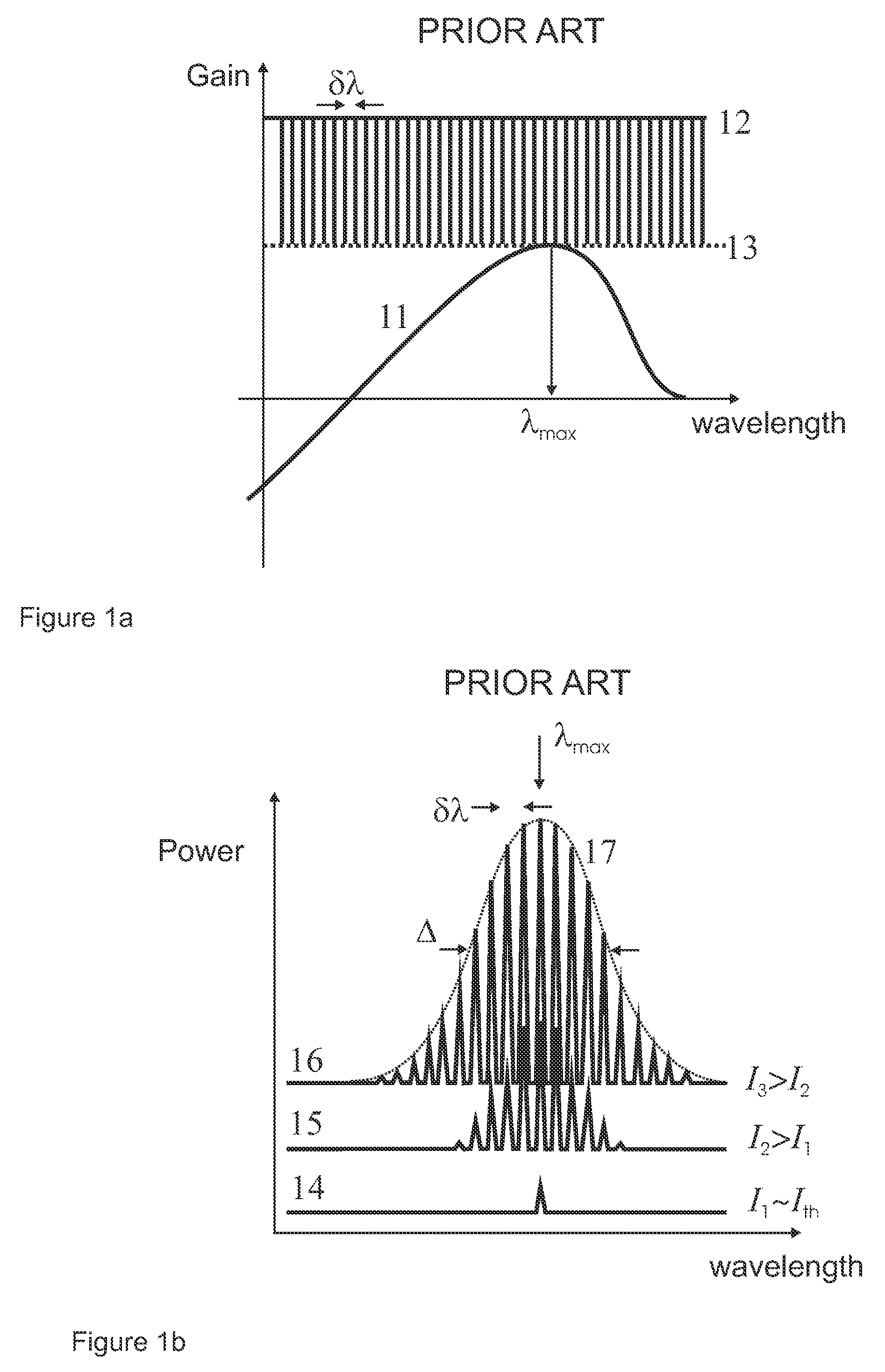
Although the spectral range of emission can be very large (e.g. several hundred nanometers), such devices are usually not very compact.
However, these devices are typically characterized by low efficiency compared to a laser device, and their output power is typically low.
Therefore, when used as an optical source for a WDM system, a LED or a SLED only provides limited power per spectral channel of the WDM system.
This solution, however, suffers from complexity in the fabrication method, which exploits post-growth modification of bandgap properties by rapid thermal annealing, as disclosed in U.S. Pat. No. 6,611,007.
One disadvantage of prior art multi-wavelength laser arrays is that an optical source for an N-channel WDM system should include at least N laser devices.
This results in additional complexity in fabrication and additional expense.

Method used


Image

  • Laser source with broadband spectrum emission
  • Laser source with broadband spectrum emission
  • Laser source with broadband spectrum emission

Examples


embodiment

PREFERRED EMBODIMENT

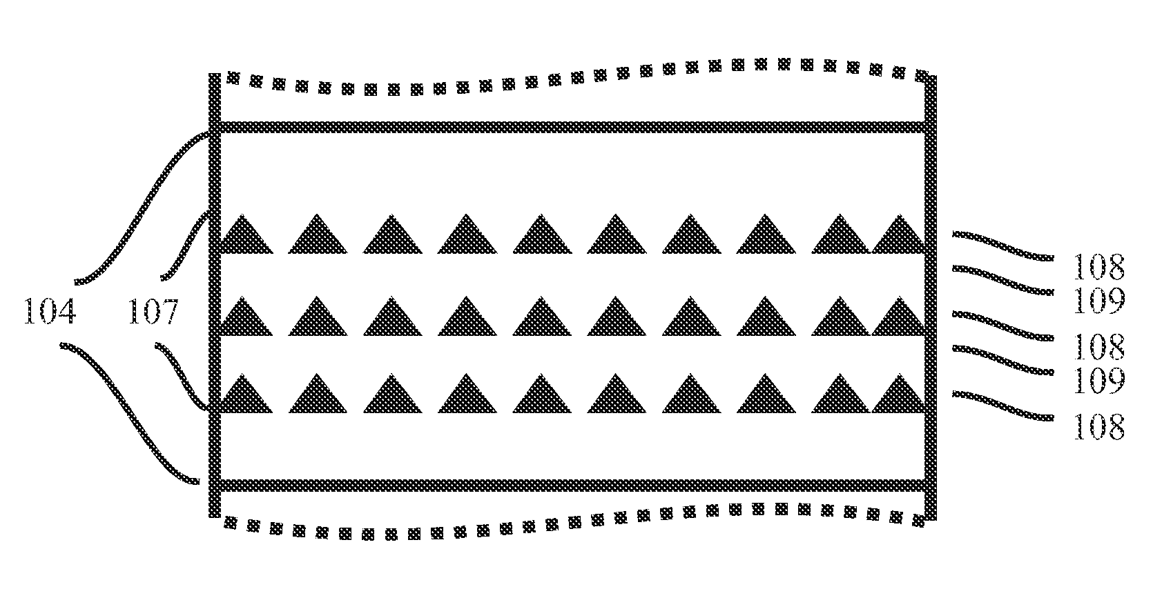
[0149]FIG. 10a shows a layered structure 101 of a quantum dot laser, preferably grown on an n+ doped substrate 102, including layers in the following order: a n-doped first cladding layer 103, a waveguiding layer 104, a p-doped second cladding layer 105, and a p+ contact layer 106, in one embodiment of the present invention. In one example, the layers are preferably an n+ doped GaAs substrate 102, an n-AlGaAs first cladding layer 103, a GaAs waveguiding layer 104, a ρ-Δ GaAs second cladding layer 105, and a p+ GaAs contact layer 106, respectively. The waveguiding layer 104 also plays the role of a matrix in which the active layer 107 is embedded. As illustrated in FIG. 10b, the active layer 107 is preferably formed by the successive deposition of several planes 108 of quantum dots separated by spacer layers 109, which are made of GaAs in this example. Each quantum dot plane preferably represents a plane of Stranski-Krastanow self-organized quantum dots embodied i...


PUM


Abstract

A quantum dot laser operates on a quantum dot ground-state optical transition. The laser has a broadband (preferably ≧15 nm) spectrum of emission and a high output power (preferably ≧100 mW). Special measures control the maximum useful pump level, the total number of quantum dots in the laser active region, the carrier relaxation to the quantum dot ground states, and the carrier excitation from the quantum dot ground states. In one embodiment, a spectrally-selective loss is introduced into the laser resonator in order to suppress lasing on a quantum dot excited-state optical transition, thereby increasing the bandwidth of the emission spectrum.

Description

[0001]This application claims inventions which were disclosed in Provisional Application No. 60 / 745,641, filed Apr. 26, 2006, entitled “LASER SOURCE WITH BROADBAND SPECTRUM EMISSION” and Provisional Application No. 60 / 863,443, filed Oct. 30, 2006, entitled “LASER SOURCE WITH BROADBAND SPECTRUM EMISSION”. The benefit under 35 USC § 119(e) of the U.S. provisional applications is hereby claimed, and the aforementioned applications are hereby incorporated herein by reference.[0002]This is also a continuation-in-part of co-pending patent application Ser. No. 11 / 295,943, filed Dec. 7, 2005, entitled “LASER SOURCE WITH BROADBAND SPECTRUM EMISSION”. The aforementioned application is hereby incorporated herein by reference.BACKGROUND OF THE INVENTION[0003]1. Field of the Invention[0004]This invention pertains to semiconductor lasers and, more specifically, to semiconductor lasers having a broad spectrum of emission.[0005]2. Description of Related Art[0006]Although narrow-band spectral output...

Claims


Application Information

Patent Timeline
Patent Type & Authority Patents(United States)
IPC IPC(8): H01S5/00
CPCB82Y20/00H01S5/341H01S5/0078H01S5/0657H01S5/1096H01S5/141H01S5/3412H01S2301/04
Inventor KOVSH, ALEXEYGUBENKO, ALEXEYZHUKOV, ALEXEYLIVSHITS, DANIILKRESTNIKOV, IGOR
Owner INNOLUME
Learn More