Deflector mirror with regions of different flexural rigidity
a deflector mirror and region technology, applied in the field of microoptical systems, can solve the problems of deflecting, degrading the optical characteristics of the reflection light of the mirror, and inertia being a great obstacle to drive speed, and achieve the effects of good optical characteristics, superior silence and power saving
- Summary
- Abstract
- Description
- Claims
- Application Information
AI Technical Summary
Benefits of technology
Problems solved by technology
Method used
Image
Examples
first embodiment
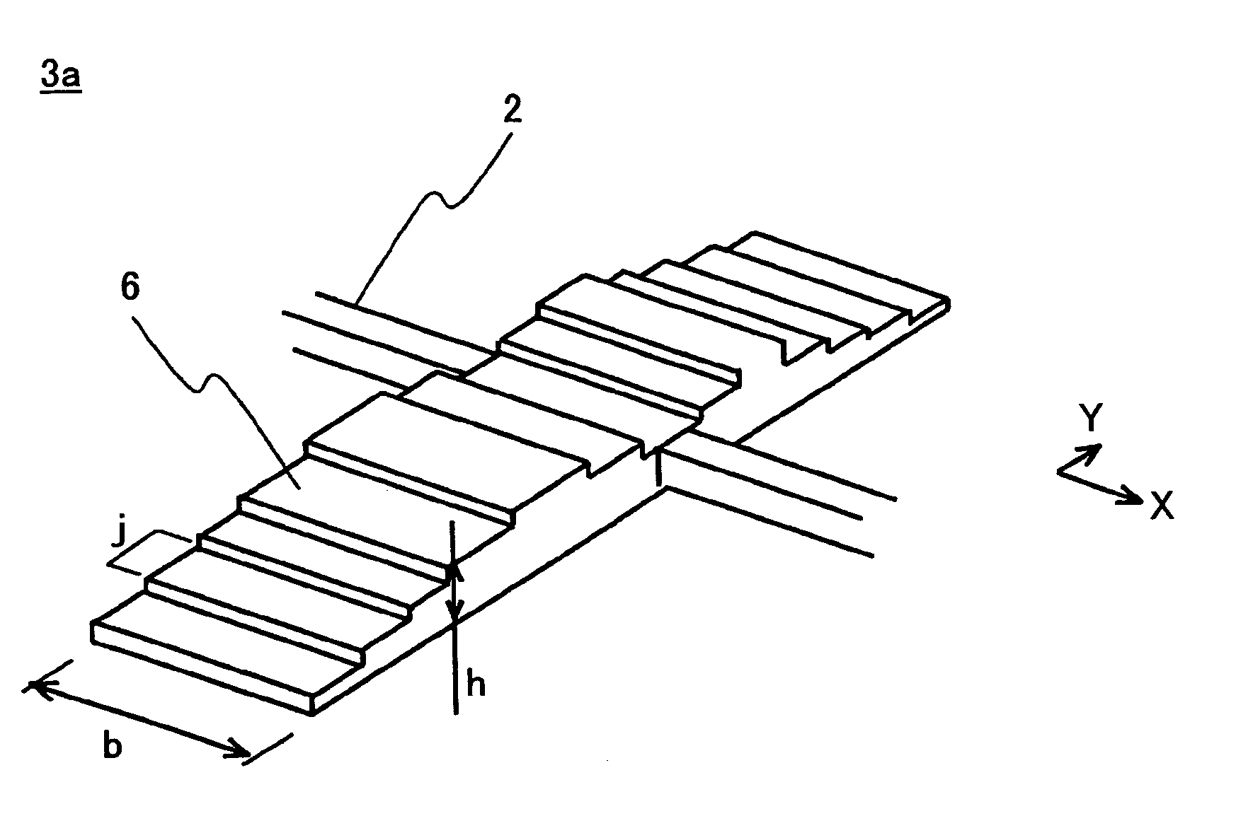
[0115]FIG. 7 is a diagram illustrating a mirror substrate 3a according to a first embodiment of the present invention. According to the first embodiment, step-like multiple regions 6 are provided on the bottom side of the mirror substrate 3 so that the flexural rigidity distribution 4 illustrated in FIG. 5 is realized. That is, an optimum flexural rigidity distribution for reducing dynamic deflection can be set by varying the thickness of the mirror substrate 3a. The step-like multiple regions 6 are formed of a silicon member.
[0116]Letting the geometrical moment of inertia in each region j of the mirror substrate 3a of FIG. 7 be Ixxj, the geometrical moment of inertia in each region j is given by the following equation:
Ixxj=bh3 / 12, (2)
where b is the width of the region j of the mirror substrate 3a, and h is the thickness of the region j of the mirror substrate 3a.
[0117]Letting the bending moment in each of the step-like regions j obtained in FIG. 5 be Mxj, the dynamic deflection δ...
second embodiment
[0119]FIG. 8A is a diagram illustrating a mirror substrate 3b according to a second embodiment of the present invention. In the second embodiment, multiple recesses 7 are formed on the bottom side of the mirror substrate 3. The multiple recesses 7 are formed of a silicon member. FIG. 8B is a cross-sectional view of the mirror-substrate 3b of FIG. 8A taken along the line B-B. The multiple recesses 7 are formed of multiple ribs 8 and a bottom plate part 9. In the second embodiment, the size of the recess 7 differs between the regions j so as to realize the flexural rigidity distribution 4 illustrated in FIG. 5. That is, an optimum flexural rigidity distribution for reducing dynamic deflection can be set by causing the size of the recess 7 to differ between the regions j.
[0120]It is assumed that the geometrical moment of inertia in each region j is Ixxj. The geometrical moment of inertia Ixxj is obtained by dividing the cross section B-B of each region j of the mirror substrate 3b into...
third embodiment
[0125]FIG. 9 is a diagram illustrating a first deflector mirror according to a third embodiment of the present invention. The deflector mirror of FIG. 9 includes a mirror substrate 20 and a substrate 21. Flexural rigidity is set for each point of the mirror substrate 20 by the method illustrated in the first or second embodiment. An external force exerted on the mirror substrate 20 is caused by an electrostatic force exerted between comb-teeth-like movable electrodes 23 formed on the free ends of the mirror substrate 20 and comb-teeth-like fixed electrodes 24 formed on the inner sides of the substrate 21 corresponding to the free ends of the mirror substrate 20. The substrate 21 includes a first Si member 25 and a second Si member 26 joined through a silicon oxide film (an insulating film) 27. An opening 28 is formed in the first Si member 25 by anisotropic etching. The mirror substrate 20 and a torsion rotary shaft 22 are formed in the second Si member 26 by a semiconductor process...
PUM
 Abstract
Description
Claims
Application Information
 - R&D
- Intellectual Property
- Life Sciences
- Materials
- Tech Scout
- Unparalleled Data Quality
- Higher Quality Content
- 60% Fewer Hallucinations
Browse by: Latest US Patents, China's latest patents, Technical Efficacy Thesaurus, Application Domain, Technology Topic, Popular Technical Reports.
© 2025 PatSnap. All rights reserved.Legal|Privacy policy|Modern Slavery Act Transparency Statement|Sitemap|About US| Contact US: help@patsnap.com


