
Reticle and optical proximity correction method

a technology of optical proximity and correction method, applied in the field of retina and optical proximity correction (opc) method, can solve the problems of unfavorable light transmission, unfavorable lithography process flexibility, and generation of micro-loading effect, so as to improve the flexibility of lithography process and reduce cost

Active Publication Date: 2009-05-05
MARLIN SEMICON LTD
View PDF4 Cites 136 Cited by
  • Summary
  • Abstract
  • Description
  • Claims
  • Application Information

AI Technical Summary

Benefits of technology

[0007]It is therefore an object of the claimed invention to provide a reticle and an OPC method to reduce the cost and to improve the flexibility of lithography process.

Problems solved by technology

This uneven distribution causes an uneven light transmittance in the exposure process, and therefore generates micro-loading effect.
The micro-loading effect leads to pattern deviations.
Since the manufacturing cost of a reticle is high, the conventional OPC method dramatically increases the cost of lithography process.

Method used


Image

  • Reticle and optical proximity correction method
  • Reticle and optical proximity correction method
  • Reticle and optical proximity correction method

Examples


Embodiment Construction

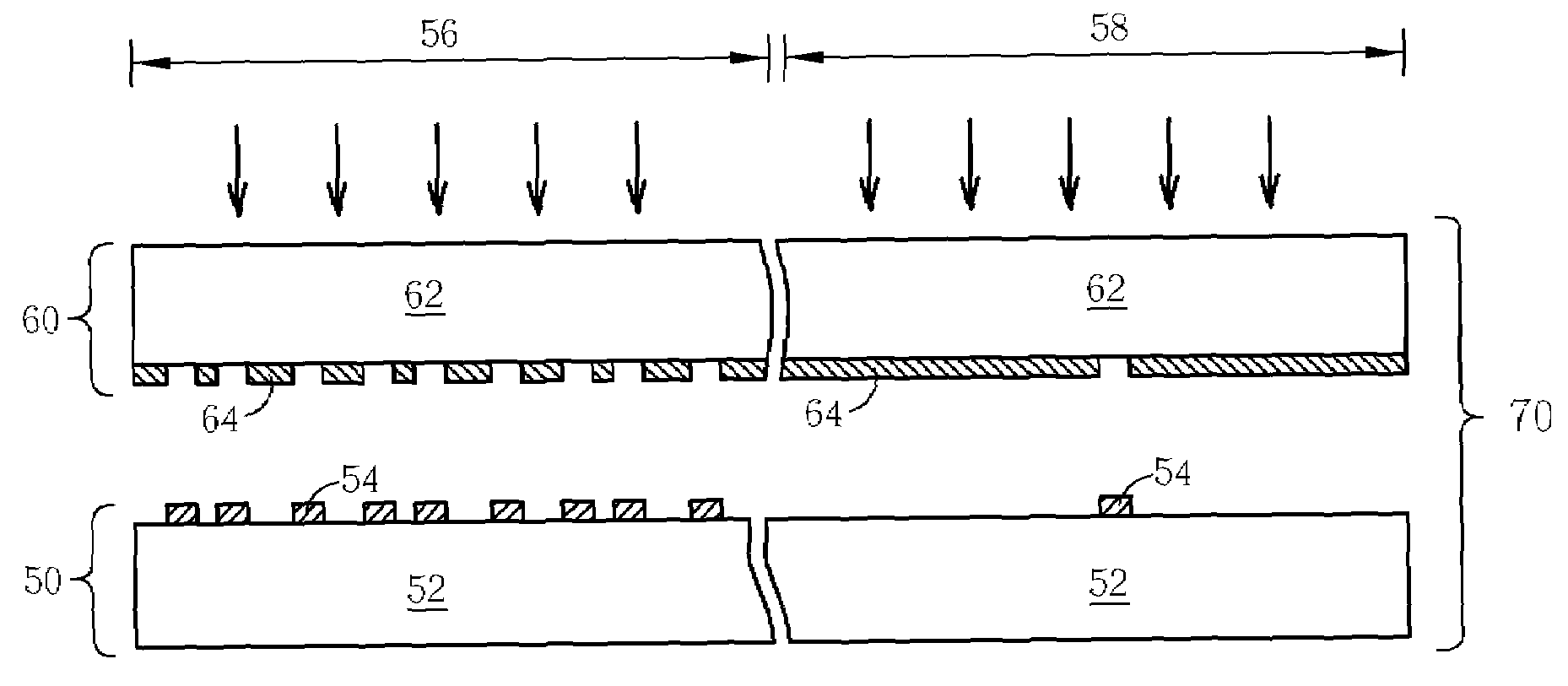
[0021]With reference to FIG. 3, FIG. 3 is a flow chart of an OPC method of the present invention. As shown in FIG. 3, the OPC method of the present invention includes the steps of:

[0022]Step 30: Start;

[0023]Step 32: Provide a primary mask having a primary pattern;

[0024]Step 34: Perform a convolution process to generate a correction pattern substantially complementary to the primary pattern;

[0025]Step 36: Form an assist mask having the correction pattern;

[0026]Step 38: Form a reticle by overlapping the primary mask and the assist mask, the light transmittance of the correction pattern being adjustable so as to equalize the light intensity distribution of the primary mask;

[0027]Step 40: End.

[0028]It can be seen that the OPC method of the present invention combines an assist mask with a primary mask to form a reticle. The primary mask has a primary pattern disposed thereon which is the circuit layout to be transferred into a photoresist layer, while the assist mask has a correction pat...


PUM

PropertyMeasurementUnit
optical proximity correctionaaaaaaaaaa
light transmittanceaaaaaaaaaa
light intensityaaaaaaaaaa

Abstract

An OPC method includes providing a primary mask having a primary pattern, forming an assist mask having a correction pattern substantially complementary to the primary pattern, and forming a reticle by overlapping the primary mask and the assist mask. The light transmittance of the correction pattern is adjustable so as to equalize the light intensity distribution of the primary mask.

Description

BACKGROUND OF THE INVENTION[0001]1. Field of the Invention[0002]The present invention relates to a reticle and an optical proximity correction (OPC) method, and more particularly, to an OPC method that uses a reticle incorporating an assist mask with a primary mask.[0003]2. Description of the Prior Art[0004]In semiconductor fabrications, quality of lithography process is critical to yield of semiconductor processes. In a lithography process, integrated circuit layout pattern disposed on a reticle (photo mask) is transferred into a photoresist layer coated on a material to be patterned. The patterned photoresist layer is then used as a hard mask to etch the material so as to form the integrated circuit layout in the material. By repeatedly patterning different material layers on a semiconductor wafer, integrated circuit is therefore fabricated.[0005]In a lithography process, proximity effect has been observed. The proximity effect can be divided into two groups: optical proximity eff...

Claims


Application Information

Patent Timeline
Patent Type & Authority Patents(United States)
IPC IPC(8): G03F1/00
CPCG03F1/144G03F1/36G03F1/32G03F1/62
Inventor ZHOU, WEN-ZHANYU, JINSEE, KAI-HUNG ALEX
Owner MARLIN SEMICON LTD
Learn More